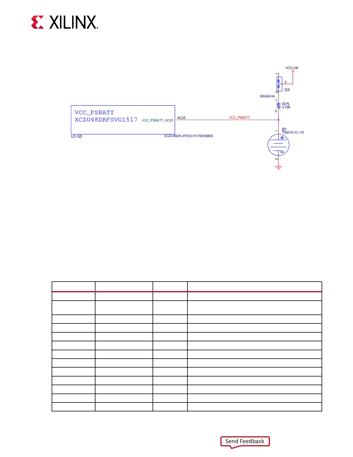
Figure 5: Encryption Key Battery Backup Circuit
The Seiko TS621E rechargeable 1.5V lithium buon-type baery B1 is soldered to the board
with the posive output connected to the ZU48DR RFSoC U1 VCC_PSBATT pin AE29. The
baery supply current IBATT specicaon is 150 nA maximum when board power is o. B1 is
charged from the VCC1V8 1.8V rail through a series diode with a typical forward voltage drop of
0.38V and 4.7 ΩK current limit resistor. The nominal charging voltage is 1.42V.
I/O Voltage Rails
The ZU48DR RFSoC PL I/O bank voltages on the ZCU208 board are listed in the following table.
Table 6: I/O Voltage Rails
ZU48DR Power Net Name Voltage Connected To
PL Bank 64 VCC1V2 1.2V PL_C0_DDR4_DQ[0:31]
PL Bank 65 VCC1V2 1.2V PL_C0_DDR4_ADDR/CTL, SYSMON_SDA/SCL,
MSP430_GPIO[0:3]
PL Bank 66 VADJ_FMC
1
1.8V FMCP_HSPC LA BUS [17:33]
PL Bank 67 VADJ_FMC
1
1.8V FMCP_HSPC LA BUS [00:16]
PL Bank 68 VCCIV2 1.2V PL_C1_DDR4_DQ[0:31]
PL_Bank 69 VCC1V2 1.2V PL_C1_DDR4_ADDR/CTL, 8A34001_GPIO[0:15]
PL Bank 84 VCC1V8 1.8V ADCIO[00:15], GPIO_DIP_SW[0:7]
PL Bank 87 VCC1V8 1.8V DACIO[0:15]
PL Bank 88 VCC1V8 1.8V SFP[0:3]_TX_DISABLE_B, CPU_RESET
PL Bank 89 VCC1V8 1.8V UART2, PL_I2C0/1, CLK104 I/F, CLK_100, GPIO_SW[N,W,C,E,S]
PS Bank 500 VCC1V8 1.8V QSPI LWR/UPR, PS_GPIO2, MIO_I2C0/1, UART0, MIO_LED/PB
PS Bank 501 VCC1V8 1.8V PMU_INPUT, PMU_GPO[0:5], SDIO I/F, PS_GPIO1
PS Bank 502 VCC1V8 1.8V USB (3.0) I/F, ENET I/F
Chapter 3: Board Component Descriptions
UG1410 (v1.0) July 8, 2020 www.xilinx.com
ZCU208 Board User Guide 24

 Loading...


