○ IN1: Unused
○ IN2: Unused
○ FB_IN: Unused
• Outputs:
○ OUT0: 27 MHz
○ Enabled, LVDS 3.3 V
○ OUT1: Unused
○ OUT2: 26 MHz
○ Enabled, LVDS 3.3 V
○ OUT3: 125 MHz
○ Enabled, LVDS 3.3 V
○ OUT4: 100 MHz
○ Enabled, HCSL 3.3 V
○ OUT5: 100 MHz
○ Enabled, LVDS 3.3 V
○ OUT6: 125 MHz
○ Enabled, LVDS 3.3 V
○ OUT7: 74.25 MHz [ 74 + 1/4 MHz ]
○ Enabled, LVDS 3.3 V
○ OUT8: Unused
○ OUT9: 33.3333333333333333... MHz [ 33 + 1/3 MHz ]
○ Enabled, LVCMOS In-phase 1.8V
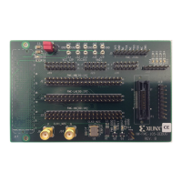
Programmable User SI570 Clocks
[Figure 2, callouts 11 and 12]
The ZCU208 board has three I2C programmable SI570 low-jier 3.3V LVDS dierenal
oscillators, two assigned to the DDR4 component memory interface banks (Bank 65 I/F C0: U47
and Bank 69 I/F C1: U130) and one assigned to GTY131 (U48).
On power-up the user clocks default to a pre-programmed output frequency: DDR4 I/F U47 and
U130 to 300.000 MHz and GTY I/F U48 to 156.250 MHz.
Chapter 3: Board Component Descriptions
UG1410 (v1.0) July 8, 2020 www.xilinx.com
ZCU208 Board User Guide 45

 Loading...