○ PS MIO[64:77]: Ethernet RGMII
• PL I/O connecons
○ PL user DIP switch (8-posion)
○ PL user pushbuons (5, geographic N, S, E, W, C)
○ PL CPU reset pushbuon
○ PL user green LEDs (24)
• Security—PSBATT buon baery backup
• SYSMON header
• Operaonal switches (power on/o, PS_PROG_B, boot mode DIP switch)
• Operaonal status LEDs (INIT, DONE, PS STATUS, PGOOD)
• Power management
• System controller (MSP430)
The ZCU208 provides a rapid prototyping plaorm that uses the XCZU48DR-2FSVG1517
device. The ZU48DR contains many useful processor system (PS) hard block peripherals exposed
through the mul-use I/O (MIO) interface and a variety of FPGA programmable logic. The
following table lists a brief summary of the resources available within the ZU48DR. Feature set
overview, descripon, and ordering informaon is provided in the Zynq UltraScale+ RFSoC Data
Sheet: Overview (DS889).
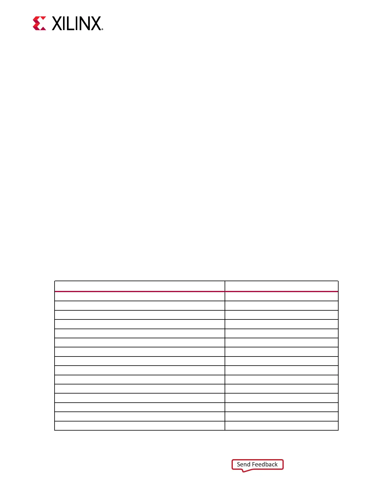
Table 1: Zynq UltraScale+ RFSoC ZU48DR Features and Resources
Feature Resource Count
SD-FEC 8
14-bit 5.0 GSPS ADC RF-DAC with DDC 8
14-bit 10 GSPS RF-DAC with DUC 8
APU: Quad-core Arm
®
Cortex™-A53 MPCore with CoreSight™ 1
RTPU: Dual-core Arm
®
Cortex™-R5F MPCore with CoreSight 1
HD I/O 96
HP I/O 312
MIO banks 3 banks, total of 78 pins
PS GTR 6 Gb/s transceivers 4 PS-GTRs
PL GTY 28 Gb/s transceivers 16 GTYs
System logic cells 930, 300
CLB flip-flops 850, 560
CLB LUTs 425, 280
Maximum distributed RAM (Mb) 13.0
Block RAM blocks 1080 (38 Mb)
Chapter 1: Introduction
UG1410 (v1.0) July 8, 2020 www.xilinx.com
ZCU208 Board User Guide 9

 Loading...


