EasyManua.ls Logo

Abov MC96F6432Q User Manual

Default Icon
327 pages
To Next Page IconTo Next Page
To Previous Page IconTo Previous Page
Page #248 background imageLoading...
Page #248 background image
MC96F6432
248 June 22, 2018 Ver. 2.9
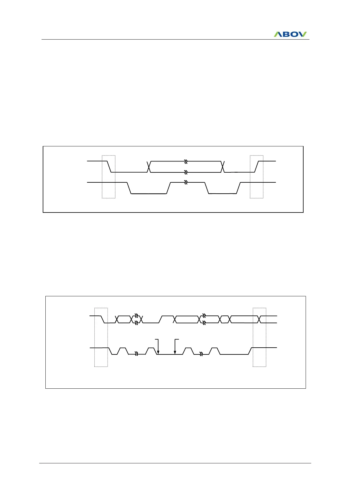
11.13.16 USI1 I2C Start / Repeated Start / Stop
One master can issue a START (S) condition to notice other devices connected to the SCL1, SDA1 lines that it
will use the bus. A STOP (P) condition is generated by the master to release the bus lines so that other devices
can use it.
A high to low transition on the SDA1 line while SCL1 is high defines a START (S) condition.
A low to high transition on the SDA1 line while SCL1 is high defines a STOP (P) condition.
START and STOP conditions are always generated by the master. The bus is considered to be busy after
START condition. The bus is considered to be free again after STOP condition, ie, the bus is busy between
START and STOP condition. If a repeated START condition (Sr) is generated instead of STOP condition, the bus
stays busy. So, the START and repeated START conditions are functionally identical.
Figure 11.89 START and STOP Condition (USI1)
11.13.17 USI1 I2C Data Transfer
Every byte put on the SDA1 line must be 8-bits long. The number of bytes that can be transmitted per transfer
is unlimited. Each byte has to be followed by an acknowledge bit. Data is transferred with the most significant bit
(MSB) first. If a slave cant receive or transmit another complete byte of data until it has performed some other
function, it can hold the clock line SCL1 LOW to force the master into a wait state. Data transfer then continues
when the slave is ready for another byte of data and releases clock line SCL1.
Figure 11.90 Data Transfer on the I2C-Bus (USI1)
START or Repeated
START Condition
S
or
Sr
STOP or Repeated
START Condition
Sr
or
P
MSB
Acknowledgement
Signal form Slave
Acknowledgement
Signal form Slave
Byte Complete,
Interrupt within Device
Clock line held low while
interrupts are served.
1
9
1
9
ACK
ACK
SDA1
SCL1
Sr
P
SCL1
SDA1
START Condition
S
P
STOP Condition

Table of Contents

Question and Answer IconNeed help?

Do you have a question about the Abov MC96F6432Q and is the answer not in the manual?

Abov MC96F6432Q Specifications

General IconGeneral
Core8051
Flash Memory64 KB
PackageLQFP-48
PWMYes
UART1
SPI1
I2C1
CPU Speed16 MHz
GPIO Pins36
Operating Voltage2.4V to 5.5V
Timers3
Operating Temperature-40°C to 85°C
ADC12-bit, 8 channels

Summary

Block Diagram

Pin Assignment

Pin Description

Electrical Characteristics

Absolute Maximum Ratings

Specifies the absolute maximum ratings for the device, beyond which permanent damage may occur.

Recommended Operating Conditions

Outlines the recommended operating voltage and temperature ranges for reliable device performance.

DC Characteristics

Provides DC electrical characteristics including input/output voltage levels, leakage current, and pull-up resistor values.

Memory

SFR Map

I/O Ports

Interrupt Controller

Interrupt Vector Table

Provides the table of interrupt sources, their symbols, enable bits, priorities, and vector addresses.

Peripheral Hardware

Clock Generator

Describes the clock generator, its overview, block diagram, and register map for system clock control.

Basic Interval Timer

Explains the 8-bit basic interval timer, its features, block diagram, and register descriptions.

Watch Dog Timer

Details the watchdog timer, its overview, timing waveform, block diagram, and register descriptions.

Timer 0

Covers Timer 0 overview, operating modes, 8-bit timer/counter mode, PWM mode, and capture mode.

Timer 1

Explains Timer 1 overview, operating modes, 16-bit timer/counter, capture, and PPG modes.

Timer 2

Details Timer 2 overview, operating modes, 16-bit timer/counter, capture, and PPG modes.

Timer 3, 4

Describes Timer 3 and 4 overview, operating modes including 8-bit and 16-bit timer/counter, capture, and PWM modes.

SPI 2

Details the SPI 2 interface, its overview, block diagram, data transfer, SS2 pin function, and timing diagrams.

12-Bit A/D Converter

Covers the 12-bit A/D converter overview, conversion timing, block diagram, ADC operation, and registers.

USI0 (UART + SPI + I2C)

Explains the USI0 module, its overview, UART mode, SPI mode, and I2C mode operations.

USI1 (UART + SPI + I2C)

Details the USI1 module, its overview, UART mode, SPI mode, and I2C mode operations.

Power Down Operation

Overview

Introduces the power-down modes (Main-IDLE, Sub-IDLE, STOP) for minimizing power consumption.

RESET

Reset Source

Lists the five types of reset sources available for the MC96F6432.

On-chip Debug System

Flash Memory

Protection for Invalid Erase/Write

Describes methods to protect flash memory from invalid erase/write operations.

Configure Option

Related product manuals