EasyManua.ls Logo

Abov MC96F6432Q User Manual

Default Icon
327 pages
To Next Page IconTo Next Page
To Previous Page IconTo Previous Page
Page #261 background imageLoading...
Page #261 background image
MC96F6432
June 22, 2018 Ver. 2.9 261
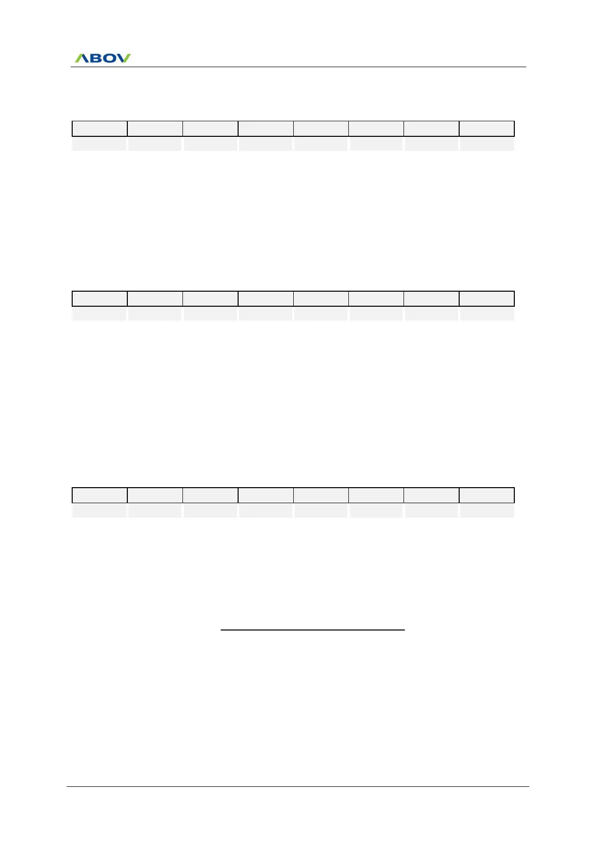
USI1DR (USI1 Data Register: For UART, SPI, and I2C mode) : F5H
7
6
5
4
3
2
1
0
USI1DR7
USI1DR 6
USI1DR 5
USI1DR 4
USI1DR 3
USI1DR 2
USI1DR 1
USI1DR 0
R/W
R/W
R/W
R/W
R/W
R/W
R/W
R/W
Initial value : 00H
USI1DR[7:0]
The USI1 transmit buffer and receive buffer share the same I/O
address with this DATA register. The transmit data buffer is the
destination for data written to the USI1DR register. Reading the
USI1DR register returns the contents of the receive buffer.
Write to this register only when the DRE1 flag is set. In SPI master
mode, the SCK1 clock is generated when data are written to this
register.
USI1SDHR (USI1 SDA Hold Time Register: For I2C mode) : F4H
7
6
5
4
3
2
1
0
USI1SDHR7
USI1SDHR6
USI1SDHR5
USI1SDHR 4
USI1SDHR 3
USI1SDHR 2
USI1SDHR 1
USI1SDHR 0
R/W
R/W
R/W
R/W
R/W
R/W
R/W
R/W
Initial value : 01H
USI1SDHR[7:0]
The register is used to control SDA1 output timing from the falling
edge of SCL1 in I2C mode.
NOTE) That SDA1 is changed after t
SCLK
X (USI1SDHR+2), in
master SDA1 change in the middle of SCL1.
In slave mode, configure this register regarding the frequency of
SCL1 from master.
The SDA1 is changed after tsclk X (USI1SDHR+2) in master
mode. So, to insure operation in slave mode, the value
t
SCLK
X (USI1SDHR +2) must be smaller than the period of SCL1.
USI1SCHR (USI1 SCL High Period Register: For I2C mode) : F7H
7
6
5
4
3
2
1
0
USI1SCHR7
USI1SCHR6
USI1SCHR5
USI1SCHR 4
USI1SCHR 3
USI1SCHR 2
USI1SCHR 1
USI1SCHR 0
R/W
R/W
R/W
R/W
R/W
R/W
R/W
R/W
Initial value : 3FH
USI1SCHR[7:0]
This register defines the high period of SCL1 when it operates in
I2C master mode.
The base clock is SCLK, the system clock, and the period is
calculated by the formula: t
SCLK
X (4 X USI1SCHR +2) where
t
SCLK
is the period of SCLK.
So, the operating frequency of I2C master mode is calculated by the following equation.
f
I2C
=
t
SCLK
X (4 X (USI1SCLR + USI1SCHR) + 4)
1

Table of Contents

Question and Answer IconNeed help?

Do you have a question about the Abov MC96F6432Q and is the answer not in the manual?

Abov MC96F6432Q Specifications

General IconGeneral
Core8051
Flash Memory64 KB
PackageLQFP-48
PWMYes
UART1
SPI1
I2C1
CPU Speed16 MHz
GPIO Pins36
Operating Voltage2.4V to 5.5V
Timers3
Operating Temperature-40°C to 85°C
ADC12-bit, 8 channels

Summary

Block Diagram

Pin Assignment

Pin Description

Electrical Characteristics

Absolute Maximum Ratings

Specifies the absolute maximum ratings for the device, beyond which permanent damage may occur.

Recommended Operating Conditions

Outlines the recommended operating voltage and temperature ranges for reliable device performance.

DC Characteristics

Provides DC electrical characteristics including input/output voltage levels, leakage current, and pull-up resistor values.

Memory

SFR Map

I/O Ports

Interrupt Controller

Interrupt Vector Table

Provides the table of interrupt sources, their symbols, enable bits, priorities, and vector addresses.

Peripheral Hardware

Clock Generator

Describes the clock generator, its overview, block diagram, and register map for system clock control.

Basic Interval Timer

Explains the 8-bit basic interval timer, its features, block diagram, and register descriptions.

Watch Dog Timer

Details the watchdog timer, its overview, timing waveform, block diagram, and register descriptions.

Timer 0

Covers Timer 0 overview, operating modes, 8-bit timer/counter mode, PWM mode, and capture mode.

Timer 1

Explains Timer 1 overview, operating modes, 16-bit timer/counter, capture, and PPG modes.

Timer 2

Details Timer 2 overview, operating modes, 16-bit timer/counter, capture, and PPG modes.

Timer 3, 4

Describes Timer 3 and 4 overview, operating modes including 8-bit and 16-bit timer/counter, capture, and PWM modes.

SPI 2

Details the SPI 2 interface, its overview, block diagram, data transfer, SS2 pin function, and timing diagrams.

12-Bit A/D Converter

Covers the 12-bit A/D converter overview, conversion timing, block diagram, ADC operation, and registers.

USI0 (UART + SPI + I2C)

Explains the USI0 module, its overview, UART mode, SPI mode, and I2C mode operations.

USI1 (UART + SPI + I2C)

Details the USI1 module, its overview, UART mode, SPI mode, and I2C mode operations.

Power Down Operation

Overview

Introduces the power-down modes (Main-IDLE, Sub-IDLE, STOP) for minimizing power consumption.

RESET

Reset Source

Lists the five types of reset sources available for the MC96F6432.

On-chip Debug System

Flash Memory

Protection for Invalid Erase/Write

Describes methods to protect flash memory from invalid erase/write operations.

Configure Option

Related product manuals