ZYNQ FPGA Development Board AX7021 User Manual
l
Amazon Store: https://www.amazon.com/alinx
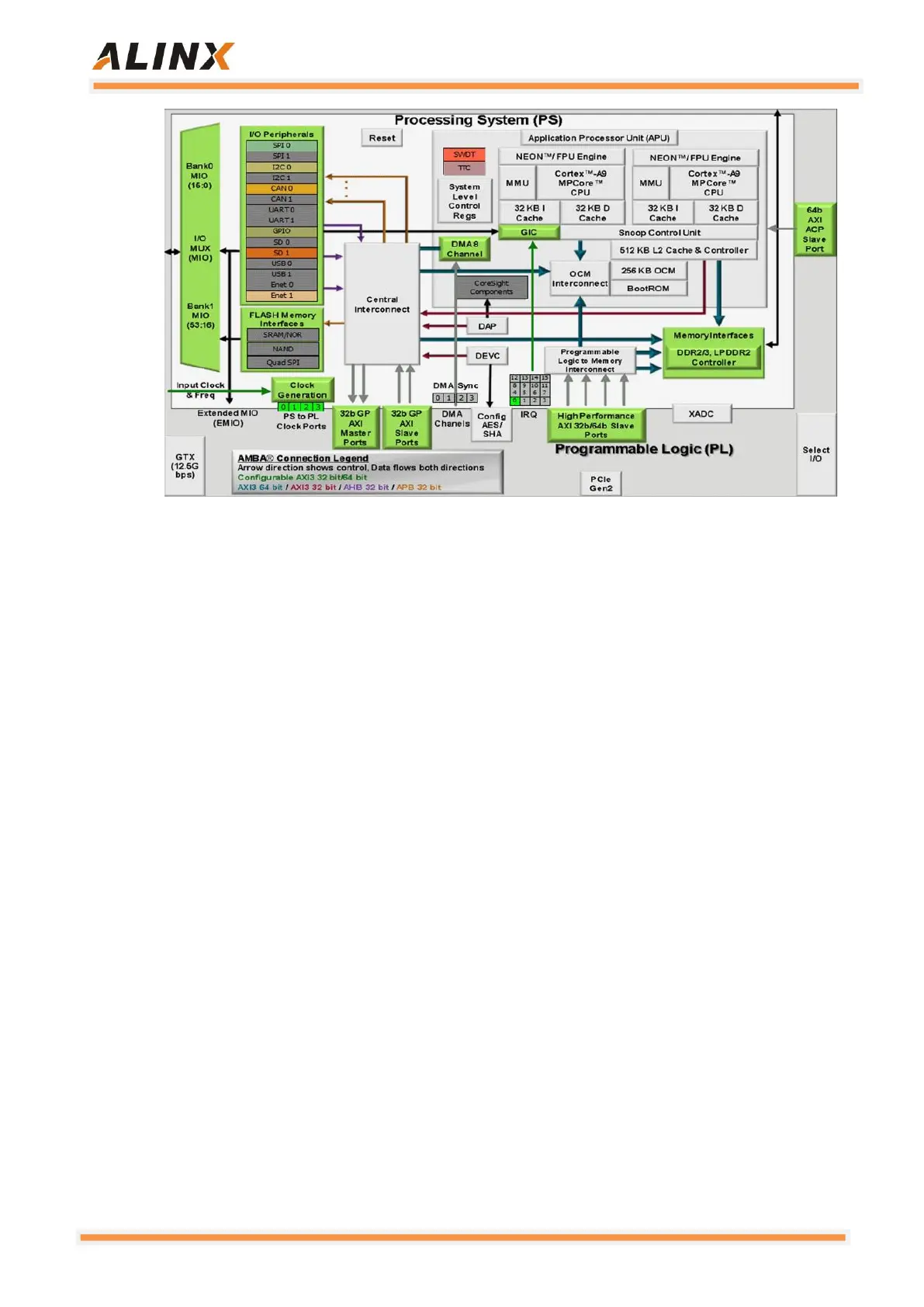
Figure 2-2-3: Overall Block Diagram of the ZYNQ7000 Chip
The main parameters of the PS system part are as follows:
ARM dual-core CortexA9-based application processor, ARM-v7
architecture, up to 1GHz
32KB level 1 instruction and data cache per CPU, 512KB level 2 cache 2
CPU shares
On-chip boot ROM and 256KB on-chip RAM
External storage interface, support 16/32 bit DDR2, DDR3 interface
Two Gigabit NIC support: divergent-aggregate DMA, GMII, RGMII,
SGMII interface
Two USB2.0 OTG interfaces, each supporting up to 12 nodes
Two CAN2.0B bus interfaces
Two SD card, SDIO, MMC compatible controllers
2 SPIs, 2 UARTs, 2 I2C interfaces
4 groups of 32bit GPIO, 54 (32+22) as PS system IO, 64 connected to
PL
High bandwidth connection within PS and PS to PL