Altera Corporation 21
Nios Development Board Reference Manual, Cyclone Edition Board Components
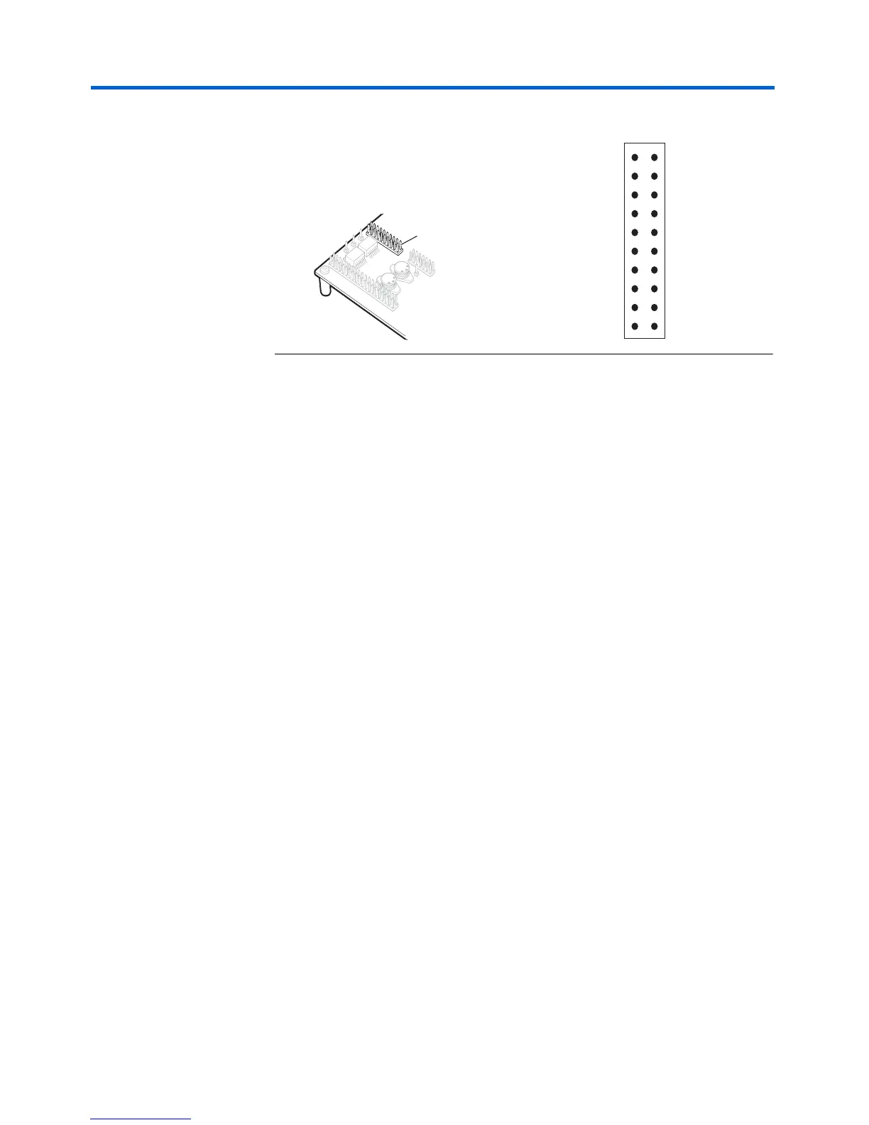
Figure 7. Expansion Prototype Connector - J13
Note to Figure 7
(1) Unregulated voltage from AC to DC power transformer.
(2) Clk from board oscillator.
(3) Clk from PLD via buffer.
(4) Clk output from protocard to PLD.
Expansion
Prototype
Connector
(PROTO2)
Headers J15, J16, and J17 collectively form the standard-footprint,
mechanically-stable connection that can be used (for example) as an
interface to a special-function daughter card.
The expansion prototype connector interface includes:
■ 41 I/O pins for prototyping. All 41 I/O pins connect to user I/O pins
on the Cyclone device. Each signal passes through analog switches
(U27, U28, U29, U30 and U31) to protect the Cyclone device from 5-V
logic levels. These analog switches are permanently enabled.
■ A buffered, zero-skew copy of the on-board OSC output (from U2).
■ A buffered, zero-skew copy of the Cyclone's phase-locked loop
(PLL)-output (from U60)
■ A logic-negative power-on-reset signal
■ Five regulated 3.3-V power-supply pins (2A total max load for both
PROTO1 & PROTO2)
■ One regulated 5-V power-supply pin (1A total max load for both
PROTO1 & PROTO2)
■ Numerous ground connections
The output logic level on the expansion prototype connector pins is 3.3V.
The power supply included wit the Nios development kit cannot supply
the maximum load current specified above.
J13
Pin 1
(1) Vunreg (U54 pin 2)
NC
+3.3V
+3.3V
(2) PROTO1_OSC(U2 pin 4)
(3) PROTO1_CLKIN (U2 pin 18)
(4) PROTO1_CLKOUT (K6)
+3.3V
+3.3V
+3.3V
GND
GND
GND
GND
GND
GND
GND
GND
GND
GND
1
3
5
7
9
11
13
15
17
19
2
4
6
8
10
12
14
16
18
20