Altera Corporation 23
Nios Development Board Reference Manual, Cyclone Edition Board Components
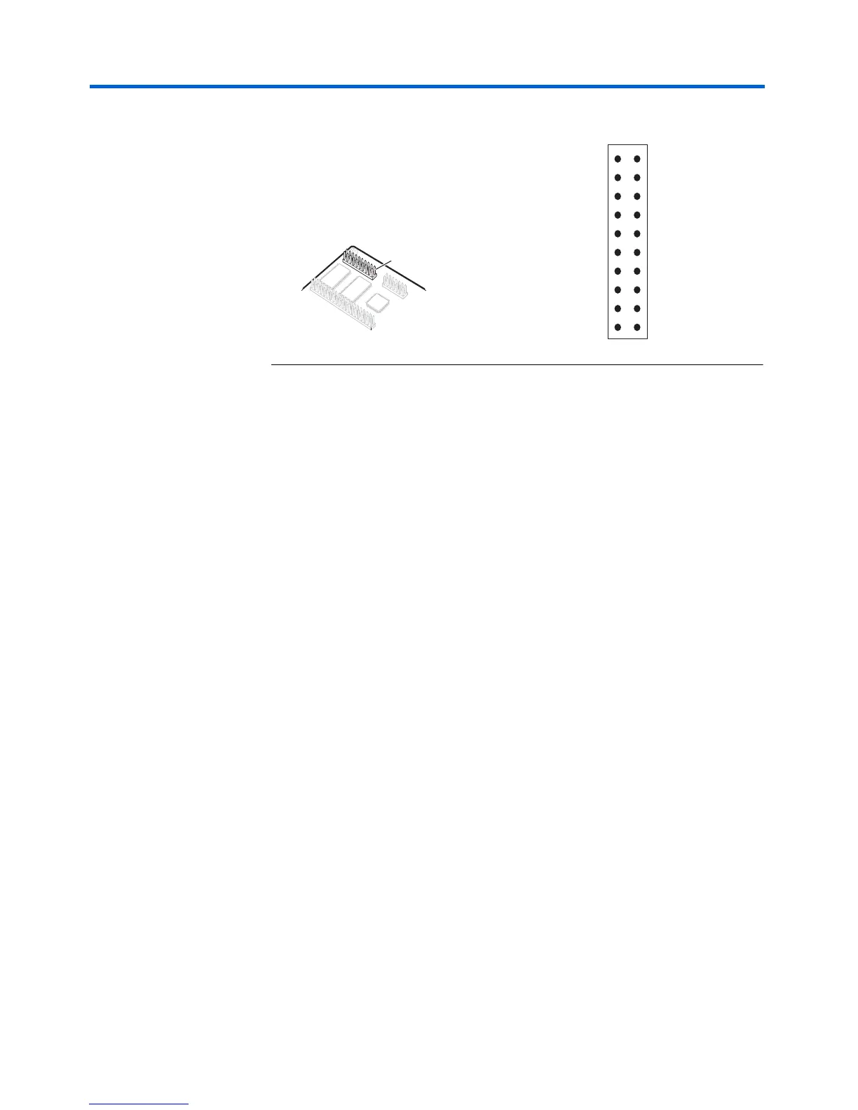
Figure 10. Expansion Prototype Connector - J17
Note to Figure 10
(1) Unregulated voltage from AC to DC power transformer.
(2) Clk from board oscillator.
(3) Clk from PLD via buffer.
(4) Clk output from protocard to PLD.
Mictor
Connector
The Mictor connector (J25) can be used to transmit up to 27 high-speed
I/O signals with very low noise via a shielded Mictor cable. J25 is used as
a debug port. Twenty five of the Mictor connector signals are used as data,
and two signals are used as clock input and clock output.
Most Mictor connector pins on J25 connect to I/O pins on the Cyclone
device (U60). For systems that do not use the Mictor connector for the
Nios OCI debug module, any on-chip signals can be routed to I/O pins
and probed at J25 via a Mictor cable. External scopes and logic analyzers
can connect to J25 and analyze a large number of signals simultaneously.
1 The Nios OCI debug module is the First Silicon Solutions Inc.
(FS2) OCI core.
f
See the Nios Development Software Tutorial for the more information about
the OCI debug module.
J17
Pin 1
(1)
Vunreg (U54 pin 2)
NC
+3.3V
+3.3V
(2)
PROTO2_OSC(U2 pin 6)
(3)
PROTO2_CLKIN (U2 pin 17)
(4)
PROTO2_CLKOUT (K14)
+3.3V
+3.3V
+3.3V
GND
GND
GND
GND
GND
GND
GND
GND
GND
GND
1
3
5
7
9
11
13
15
17
19
2
4
6
8
10
12
14
16
18
20