Altera Corporation 31
Nios Development Board Reference Manual, Cyclone Edition Board Components
Each of the upper four (4) MBbytes of flash memory are used by either the
configuration controller or the web server. Your application software may
safely use the lower half (4 MBytes) of flash memory without interfering
with FPGA configuration or web-server operation.
1 The factory-programmed reference design implements a web
server. Network settings and web pages are pre-programmed in
the flash memory, as shown in Table 10 on page 32.
w WARNING: The safe example design is provided for reference
only. Do not base your hardware or software designs on the safe
example design. Use the standard_32 example design.
User Hardware Image
At power on, or when the Reset, Config button (SW10) is pressed, the
configuration controller begins reading user configuration data out of
flash at address 0x600000. This data, and suitable control signals, are used
in an attempt to configure the FGPA. FPGA configuration data written
into this region of flash memory is conventionally called the User
Hardware Image. The web server includes documentation on how to
create your own User Hardware Image data and several facilities for
burning your User Hardware Image into flash memory.
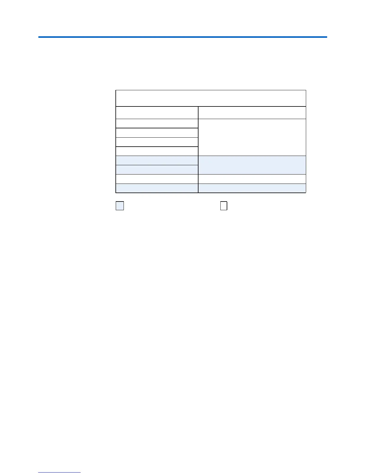
Table 9. Flash Memory Allocation
Address (hex) Flash Allocation
000000 4MB
100000
200000
300000
400000 Web Pages (2MB)
500000
600000 User Configuration Data (1 MB)
700000 Safe Configuration Data (1 MB)
Factory-programmed–
do not erase
Available for user data.