VCU118 Board User Guide 113
UG1224 (v1.5) March 15, 2023
Chapter3: Board Component Descriptions
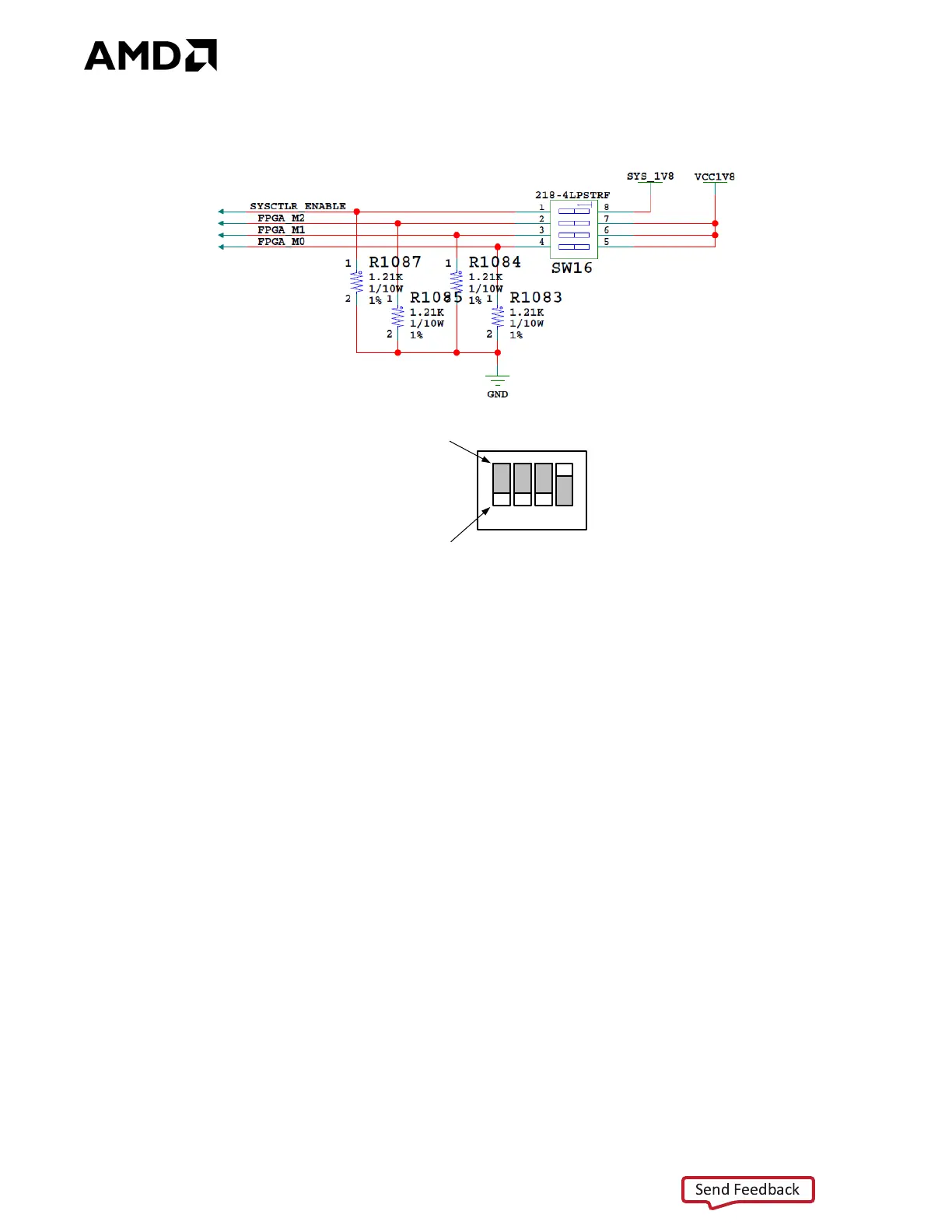
Figure 3-30 shows mode switch SW16.
The mode pins settings on SW16 determine if the Quad SPI flash is used for configuring the
FPGA. DIP switch SW16 also includes a system controller enable switch in position 1.
To obtain the fastest configuration speed, an external 90 MHz clock from the Silicon Labs
Si5335A U122 is wired to the EMCCLK pin of the FPGA on bank 65 pin AL20. This allows the
creation of bitstreams to configure the FPGA over the 8-bit datapath from the dual Quad
SPI flash memory at a maximum synchronous read rate of 90 MHz.
X-Ref Target - Figure 3-30
Figure3‐30: SW16 JTAG Settings
1
2
34
SW16
OFF Position = 0
ON Position = 1
SCE
M2
M1
M0
X18009-091818