165
7679H–CAN–08/08
AT90CAN32/64/128
15. Output Compare Modulator - OCM
15.1 Overview
Many register and bit references in this section are written in general form.
• A lower case “n” replaces the Timer/Counter number, in this case 0 and 1. However, when
using the register or bit defines in a program, the precise form must be used, i.e., TCNT0 for
accessing Timer/Counter0 counter value and so on.
• A lower case “x” replaces the Output Compare unit channel, in this case A or C. However,
when using the register or bit defines in a program, the precise form must be used, i.e.,
OCR0A for accessing Timer/Counter0 output compare channel A value and so on.
The Output Compare Modulator (OCM) allows generation of waveforms modulated with a carrier
frequency. The modulator uses the outputs from the Output Compare Unit C of the 16-bit
Timer/Counter1 and the Output Compare Unit of the 8-bit Timer/Counter0. For more details
about these Timer/Counters see “16-bit Timer/Counter (Timer/Counter1 and Timer/Counter3)”
on page 113 and “8-bit Timer/Counter0 with PWM” on page 99.
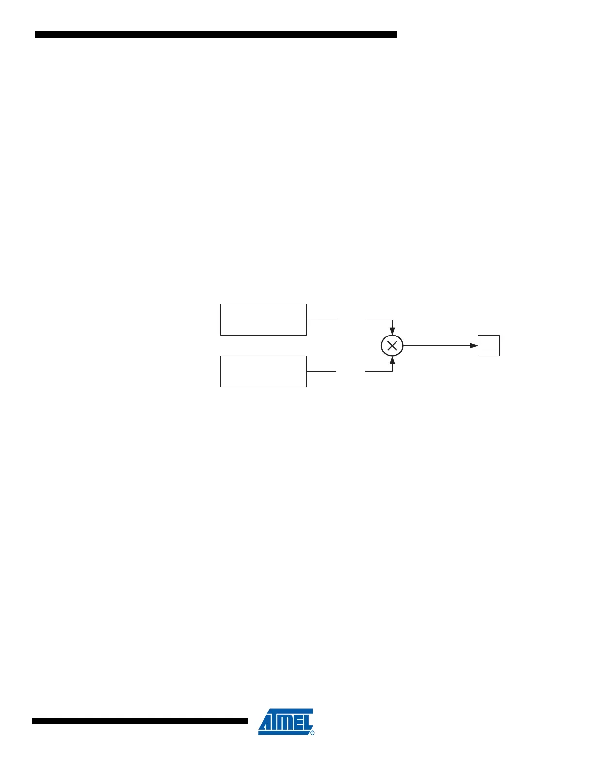
Figure 15-1. Output Compare Modulator, Block Diagram
When the modulator is enabled, the two output compare channels are modulated together as
shown in the block diagram (Figure 15-1).
15.2 Description
The Output Compare unit 1C and Output Compare unit 0A shares the PB7 port pin for output.
The outputs of the Output Compare units (OC1C and OC0A) overrides the normal PORTB7
Register when one of them is enabled (i.e., when COMnx1:0 is not equal to zero). When both
OC1C and OC0A are enabled at the same time, the modulator is automatically enabled.
When the modulator is enabled the type of modulation (logical AND or OR) can be selected by
the PORTB7 Register. Note that the DDRB7 controls the direction of the port independent of the
COMnx1:0 bit setting.
The functional equivalent schematic of the modulator is shown on Figure 15-2. The schematic
includes part of the Timer/Counter units and the port B pin 7 output driver circuit.
OC1C
Pin
OC0A / OC1C / PB7
Timer/Counter 1
Timer/Counter 0
OC0A

 Loading...


