Chapter 6
6-2
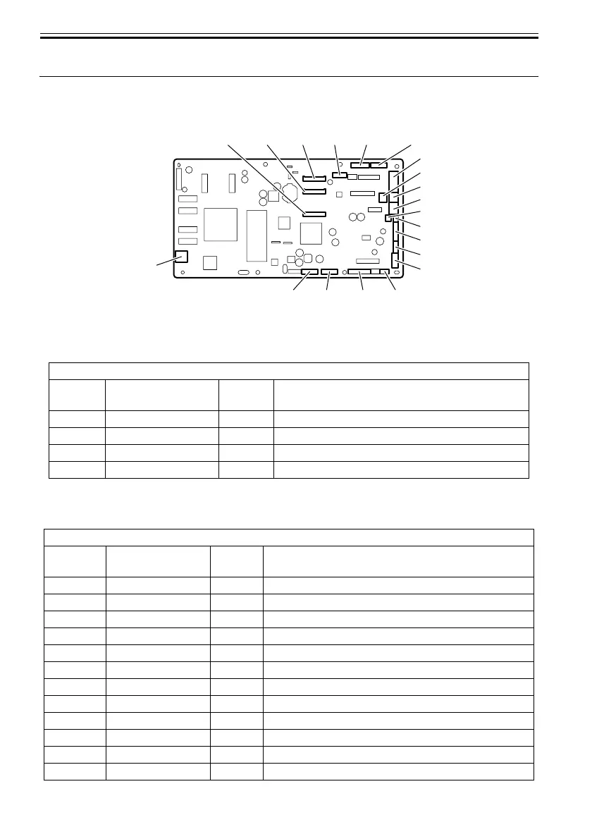
6.2 Location of Connectors and Pin Arrangement
6.2.1 Main controller PCB
0017-5653
F-6-1
T-6-1
T-6-2
J1001
Pin
Number
Signal name IN/OUT Function
1 VBUS IN USB VBUS (+5V)
2 D- IN/OUT USB data (-)
3 D+ IN/OUT USB data (+)
4 GND - USB GND
J1801
Pin
Number
Signal name IN/OUT Function
1 AFCONT OUT Normal/power saving switch signal
2 VM_ENB OUT VM enable signal
3 VMGND - GND
4 VMGND - GND
5 VM IN Power supply (+32V)
6 VM IN Power supply (+32V)
7GND -GND
8GND -GND
9GND -GND
10 RGV20(+5V) IN Power supply (+5V)
11 RGV20(+5V) IN Power supply (+5V)
12 RGV20(+5V) IN Power supply (+5V)
J1801
J2503
J3101
J3001
J3004
J2702
J2801
J1001
J2701
J2704
J2703
J2601
J3301J2502J3201J3202
J2501J3601J3602J3401