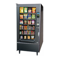
Snack - Based Troubleshooting and Repair Guide
September, 2002 Page 7 of 54 1670065
ductor ribbon cable connected at J55 of the Interface Board (see Interface Board). Tray
status and other conditions including the status of rail boards as well as all other
peripherals connected to the Interface Board are monitored here. Operational com-
mands for peripherals are sent and received via this port using a serial data stream.
NOTE:
Disruption of this data stream will result in a (TEMPORARY OUT OF SERVICE),
(ABCDEF)
OR (NONE READY) error message in the display. This condition will
continue until such time that the problem is corrected.
Pins 2-14 provide communication through IC U7 via microprocessor U1. 5 volts dc
logic circuit voltage can be measured between pins 1 and 15.
b. J33 Display PCB Connection. Pins 1 and 9 provide 5 volts dc for operation of display
console logic circuit functions. All display data, including load beeper, are controlled
through the following IC chips: U13A (octal 3-state driver), U6 (general I/O buffer),
and gate controlled U9C (OR gate). This port provides visual information concerning
the state of merchandiser, command control and diagnostics.
c. J34 Used for Sure-Vend.
d. J35 Communication Port. Reserved for future use.
e. J36 DEX Device Port. This is a serial data communication port for retrieving data
from the merchandiser by way of hand held printer or (DEX) data retrieval device. Pin
1 provides a ground reference for data transmission (pin 2), data receive (pin 3), and
return transmission signal (RTS) (pin 4). Pin 3 also acts as a communication transmis-
sion signal (CTS) and reports directly to microprocessor U1. Data transfer is con-
trolled through U14 inverter chip. 5 volts dc can be measured at pins 1 and 4 for logic
circuit operation.
NOTE:
See DEX Overview and Capabilities on page 14 for more information.
f. J37. 24 vac is supplied to pins 1 and 2 of this connector. This voltage is received from
the Transformer (see “Power Circuit” on page 6) located on power panel. The 24 vac
is rectified at bridge BR1 (bridge rectifier) and sent as 24 volt unregulated dc to vari-
ous locations on the board, and to regulator circuit REG 1. At the regulator circuit the
dc voltage is filtered and reduced to 5 vdc for use as high and low signals (on/off) for
all logic circuit functions and other on-board uses.
g. J38. Pins 1 and 2 of this connector supply output power to the Interface Board. This
24 volt unregulated dc is sent to the Interface Board at connector J-62 where it is regu-
lated (See Interface Board).
h. J39 MDB (Multi-Drop Bus) Port. Unregulated 24 volts dc at pin 6 and unregulated
dc return at pin 5 is used to power all MDB protocol capable monetary units. These
include coin mechanisms, dollar bill validators, card readers etc. (See Multi-Drop
Bus). Master data transmissions, and receiving communication is accomplished at pins
3 (transmit data) and 4 (receive data). Pins 1 and 2 supply a regulated and filtered 5
volts for monetary unit logic circuits.