Board Reference / Pins CSI mapping DSI mapping
J1001 / 7,8 Clock Data Lane 0
J1001 / 10,11 Data Lane 1 Clock
J1001 / 13,14 Data Lane 0 Data Lane 1
Table 28: MIPI Connector 1 CSI / DSI Signal Mapping - Rasperry Pi Display Lane Mapping
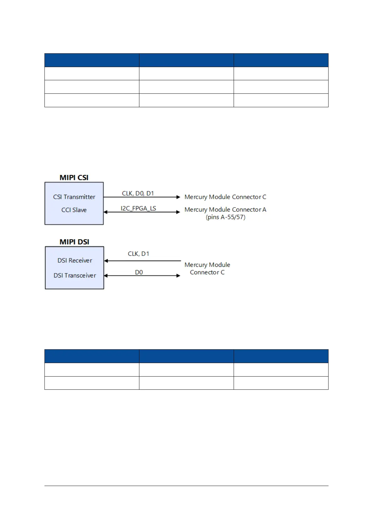
Figure 17 shows the connections for the CSI and DSI use cases. When the MIPI interface is used as CSI, the
FPGA I2C bus is used as camera control interface (CCI).
In case of a DSI interface, the pins corresponding to I2C may be used for power - please read carefully the
datasheet of the connected MIPI device to check the connectivity requirements.
Figure 16: MIPI CSI/DSI Interface with Zynq UltraScale+ Modules
When a display is used for MIPI1 interface, the FPGA I2C must be connected to MIPI0 interface (for the CCI
function) leaving the I2C MIPI1 pins available for the power connections - refer to Table 29.
The I2C for the camera interfaces may be selected via I2C_MIPI_SEL signal.
I2C_MIPI_SEL Value MIPI I2C Active I2C_SDA_MIPI1 State
0 MIPI0 VCC_3V3
1 MIPI1 I2C_SDA_FPGA_LS
Table 29: MIPI I2C Bus Selection and Connectivity Options
For use with older FPGA families that do not natively support SLVS IO standard (Zynq-7000, 7-series, Cyclone
V) hardware changes are required in order to provide proper signal termination and tap the high-speed
signals to dedicated FPGA inputs. Low-power signaling is supported only for lane 0 (D0). Clock and data 1
support only the high-speed mode.
D-0000-456-001 40 / 48 Version 02, 23.07.2020
 Loading...