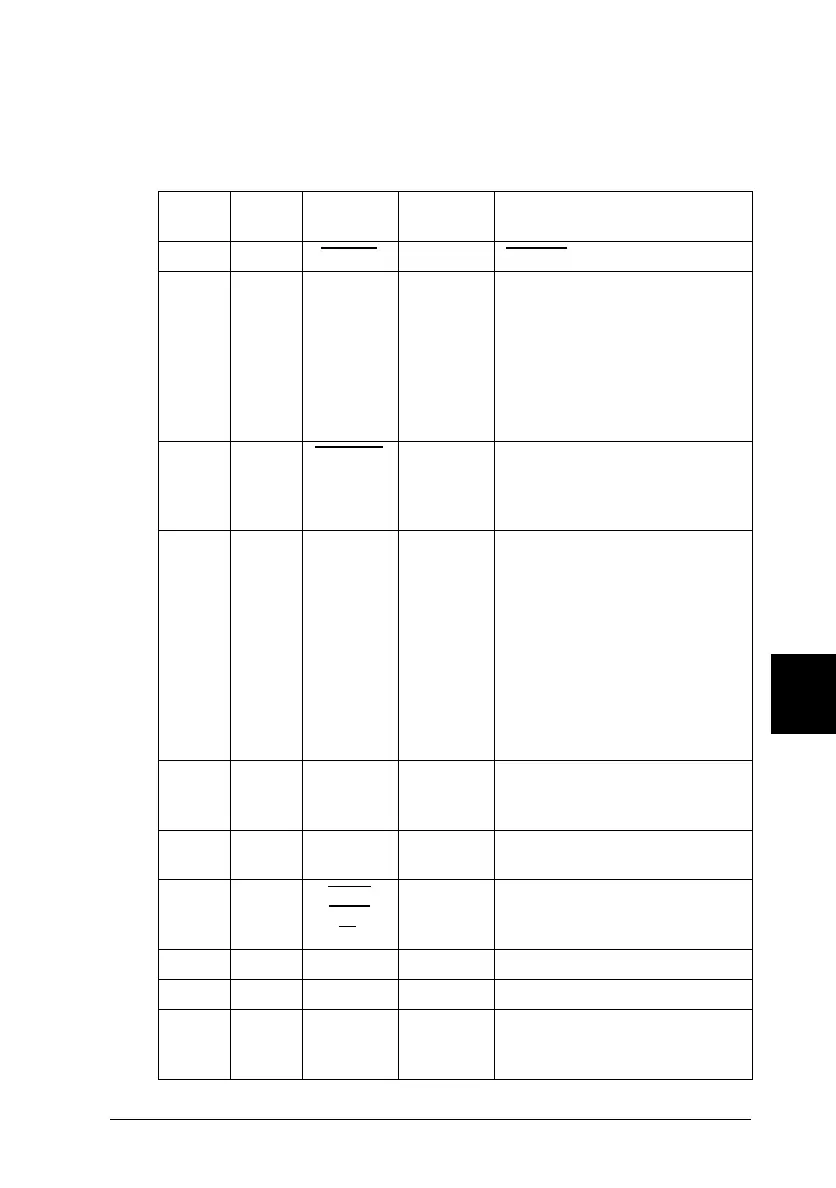
Pin assignments
The parallel interface connector pin assignments and a description of the
interface signals are shown in the table below.
Signal
Pin
Return
Pin Signal Direction Description
119
STROBE IN STROBE pulse to read data.
2
3
4
5
6
7
8
9
20
21
22
23
24
25
26
27
DATA 0
DATA 1
DATA 2
DATA 3
DATA 4
DATA 5
DATA 6
DATA 7
IN
IN
IN
IN
IN
IN
IN
IN
These signals represent
information in bits 0 to 7 of
parallel data respectively.
Each signal is at HIGH level
when data is logical 1 and
LOW when it is logical 0.
10 28
ACKNLG OUT About a 5-µs pulse. LOW
indicates data has been
received and the printer is
ready to accept more data.
11 29 BUSY OUT A HIGH signal indicates the
printer can not receive data.
The signal goes HIGH in the
following cases:
1) During data entry
(for each character)
2) During initialization
3) During self test,
demonstration, and
default-setting printing
4) During a printer-error state
12 28 PE OUT A HIGH signal indicates the
printer is in a paper-out state
or in an error state.
13 28 SLCT OUT Pulled up to +5 V through
1 kΩ resistance
14 30
AUTO
FEED
XT
IN Not used
15 - NC - Not used
16 - GND - Logic ground level
17 - CHASSIS
GND
- Printer’s chassis ground,
which is connected to the
logic ground.
D
R
Loire-p Ref. Guide
Rev.c
A5 size Appendix D
02-24-97 DR, pass 0
Specifications
D-13
 Loading...