ES720.1 - User’s Guide 71
ETAS Technical Data
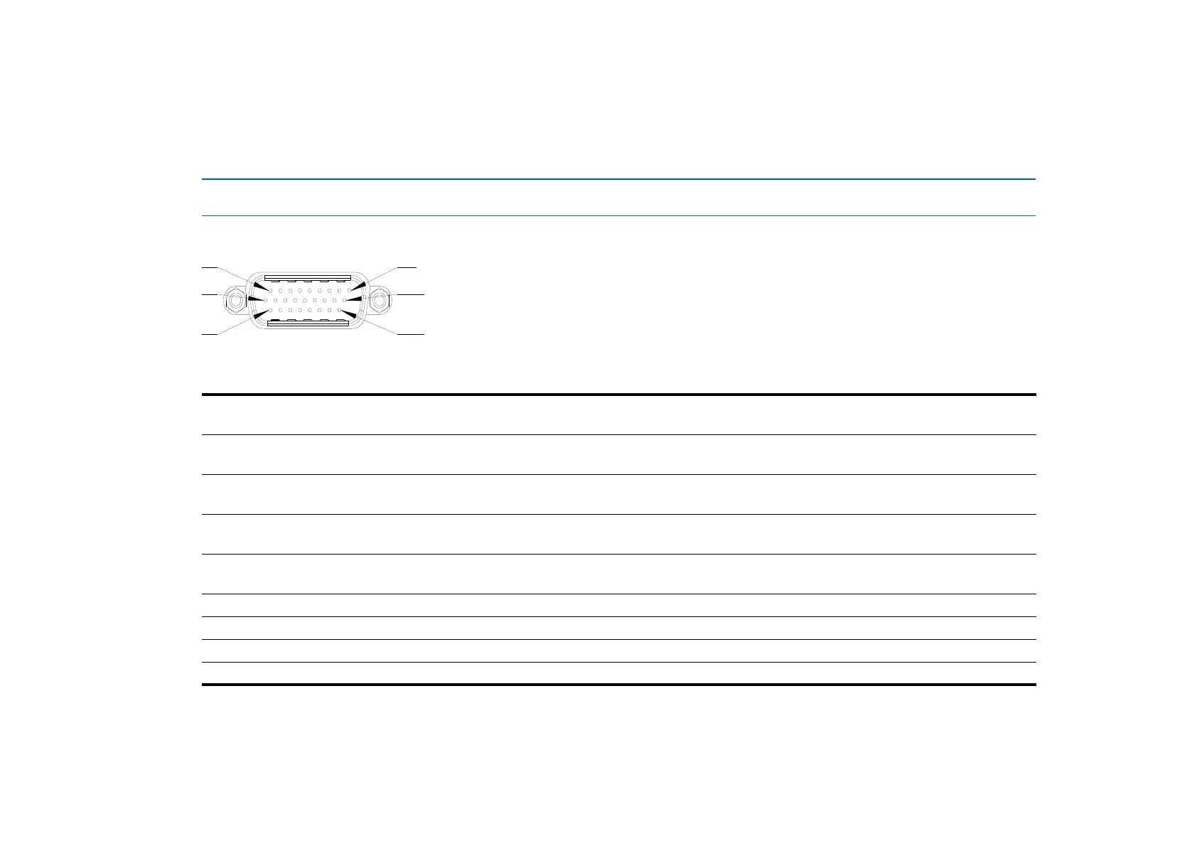
8.5.7 Interface „I/O“
Pin Assignment and Technical Data
Fig. 8-4 Interface „I/O“
All inputs and outputs of the „I/O“ interface are protected against overvoltages until +/- 32 V.
Pin Signal Type Logic I max.
[mA]
Meaning
1 OUT_1 Output 5 V 10 TTL-compatible, max. 0.5 V @ 0 mA, min. 2.5 V @ 10 mA,
can be used as INCA signal
2 OUT_2 Output 5 V 10 TTL-compatible, max. 0.5 V @ 0 mA, min. 2.5 V @ 10 mA,
can be used as INCA signal
3 OUT_3 Output 5 V 10 TTL-compatible, max. 0.5 V @ 0 mA, min. 2.5 V @ 10 mA,
can be used as INCA signal
4 OUT_4 Output 5 V 10 TTL-compatible, max. 0.5 V @ 0 mA, min. 2.5 V @ 10 mA,
can be used as INCA signal
5 GND - - - Ground
6 GND - - - Ground
7 GND - - - Ground
8 GND - - - Ground
 Loading...