EasyManuals Logo

Fibocom L860-GL-16 User Manual

Fibocom L860-GL-16
60 pages
To Next Page IconTo Next Page
To Previous Page IconTo Previous Page
Page #17 background imageLoading...
Page #17 background image
Reproduction forbidden without Fibocom Wireless Inc. written authorization - All Rights Reserved.
FIBOCOM L860-GL Series Hardware Guide Page 17 of 60
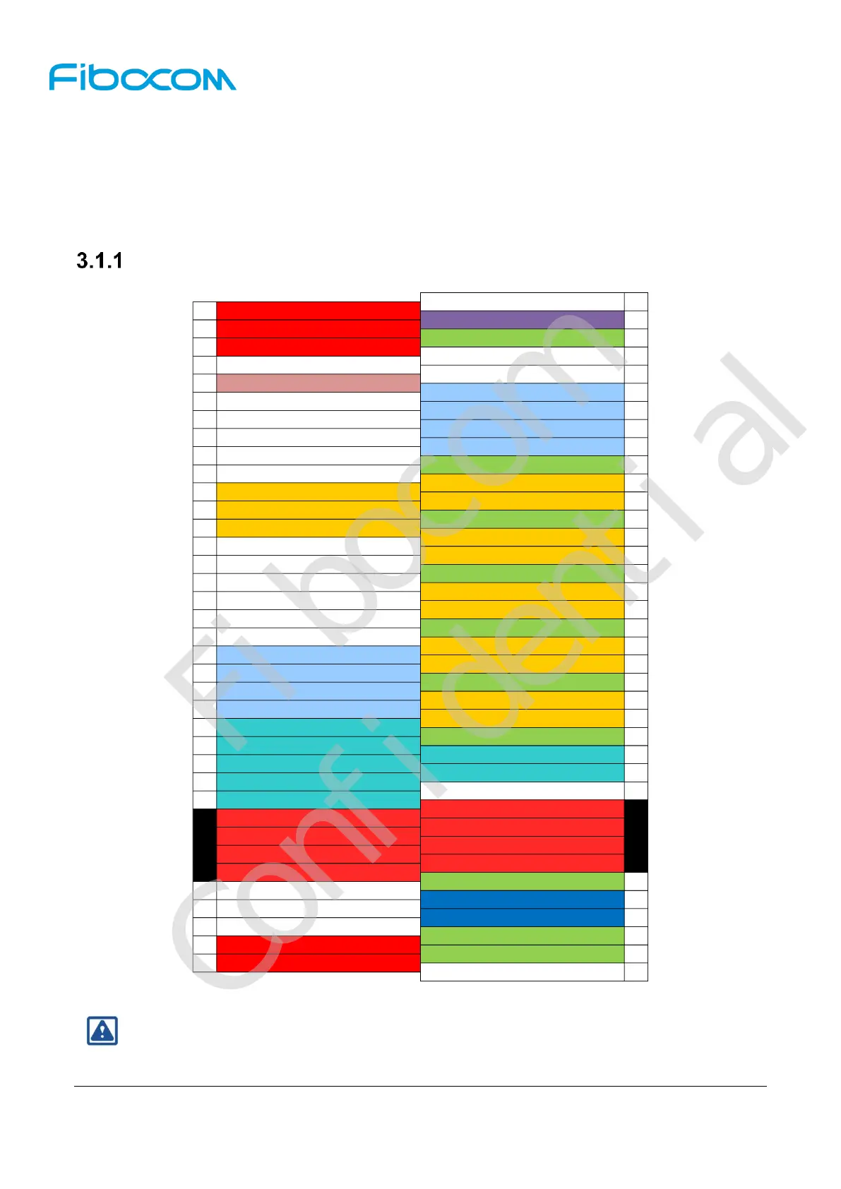
3 Application Interface
3.1 M.2 Interface
The L860 module applies standard M.2 Key-B interface, with a total of 75 pins.
Pin Map
Figure 3-1 Pin map
Note:
Pin “Notchrepresents the gap of the gold fingers.
74
72
70
68
66
64
62
60
58
56
54
52
50
48
46
44
42
40
10
8
6
4
38
36
34
32
30
28
26
24
22
2
NC
I2C_IRQ#(1.8V)
I2C_SDA(1.8V, I2C Slave/Master)
I2C_SCL(1.8V, I2C Slave/Master)
+3.3V
+3.3V
+3.3V
ANT_CONFIG(1.8V)
SIM1_DETECT(1.8V)
COEX_TXD(1.8V)
COEX_RXD(1.8V)
COEX3(1.8V)
RFE_RFFE_SDATA
Notch
LED1#(3.3V OD)
W_DISABLE1#(3.3/1.8V)
FULL_CARD_POWER_OFF#(3.3/1.8V)
+3.3V
PEWAKE# (3.3V)
CLKREQ# (3.3V)
PERST# (3.3V)
NC
20
USB D+
GND
GND
+3.3V
UIM1_RESET
UART_RX(1.8V, mux for GPIO)
W_DISABLE2#(3.3/1.8V)
ANT_TUNER_1V8(1.8V, mux for GPIO)
UART_TX(1.8V, mux for ANT_TUNER_CFG/GPIO)
Notch
USB3.0-Tx
GND
DPR(3.3/1.8V)
WOWWAN#(1.8V)
CONFIG_0
Notch
Notch
Notch
USB D-
CONFIG_2
VIO_CFG
GND
CONFIG_1
RESET#(1.8V)
ANTCTL3(1.8V)
ANTCTL2(1.8V)
ANTCTL1(1.8V)
ANTCTL0(1.8V)
GND
REFCLKP
REFCLKN
GND
PERp0
PERn0
GND
PETp0
PETn0
GND
USB3.0-Rx+
USB3.0-Rx
GND
GND
CONFIG_3
75
73
71
69
67
65
63
61
59
57
55
53
51
49
47
45
43
3
41
1
11
21
23
GPIO(1.8V)
Notch
Notch
Notch
USB3.0-Tx+
NC
UIM1_PWR
UIM1_DATA
UIM1_CLK
RFE_RFFE_SCLK
9
7
5
39
37
35
33
31
29
27
25
Fibocom
Confidential

Questions and Answers:

Question and Answer IconNeed help?

Do you have a question about the Fibocom L860-GL-16 and is the answer not in the manual?

Fibocom L860-GL-16 Specifications

General IconGeneral
BrandFibocom
ModelL860-GL-16
CategoryComputer Hardware
LanguageEnglish

Related product manuals