Reproduction forbidden without Fibocom Wireless Inc. written authorization - All Rights Reserved.
FIBOCOM L860-GL Series Hardware Guide Page 32 of 60
The extra 0.3mA is consumed on
CLKREQ# pull down
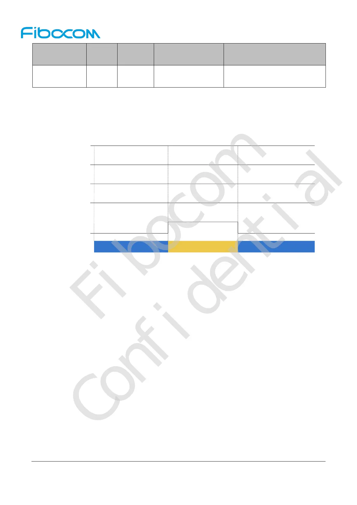
3.3.4.1 D0 L1.2
Module supports PCIe goes into D0 L1.2 state in Win10 system. The D0->D0 L1.2@S0/S0ix->D0 timing
is shown in Figure 3-10:
+3.3V
PERST#
RESET#
Module State
D0 L1.2@S0/S0ixD0 L0@S0/S0ix
FCPO#
D0 L0@S0/S0ix
CLKREQ#
Figure 3-10 D0 L1.2 timing
3.3.4.2 D3
cold
L2
Module supports PCIe goes into D3
cold
L2 state in Win10 system. The D0->D3
cold
L2@S0/S0ix
->D0 timing is shown in Figure 3-11 and Figure 3-12:
 Loading...