Reproduction forbidden without Fibocom Wireless Inc. written authorization - All Rights Reserved.
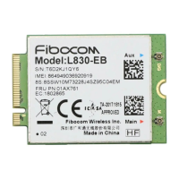
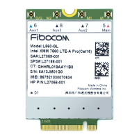
FIBOCOM L860-GL Series Hardware Guide Page 20 of 60
PCIe RX differential signal
Negative
PCIe RX differential signal
Positive
Asserted to reset module PCIe
interface default. If module went into
core dump, it will reset whole module,
not only PCIe interface.
Active low, internal pull up (10KΩ)
Asserted by device to request a PCIe
reference clock be available (active
clock state) in order to transmit data. It
also used by L1 PM Sub states
mechanism, asserted by either host or
device to initiate an L1 exit.
Active low, internal pull up (10KΩ)
PCIe reference clock signal
Negative
Asserted to wake up system and
reactivate PCIe link from L2 to L0, it
depends on system whether supports
wake up functionality.
Active low, open drain output and
should add external pull up (100KΩ) on
platform
PCIe reference clock signal, Positive
MIPI interface tunable ANT,
RFFE clock
MIPI interface tunable ANT,
RFFE data
 Loading...