3-10
CIRCUIT DESCRIPTIONS
TO A-ASIC
{If uiatog tiagefinf)
«f Ogim tnpgenngj
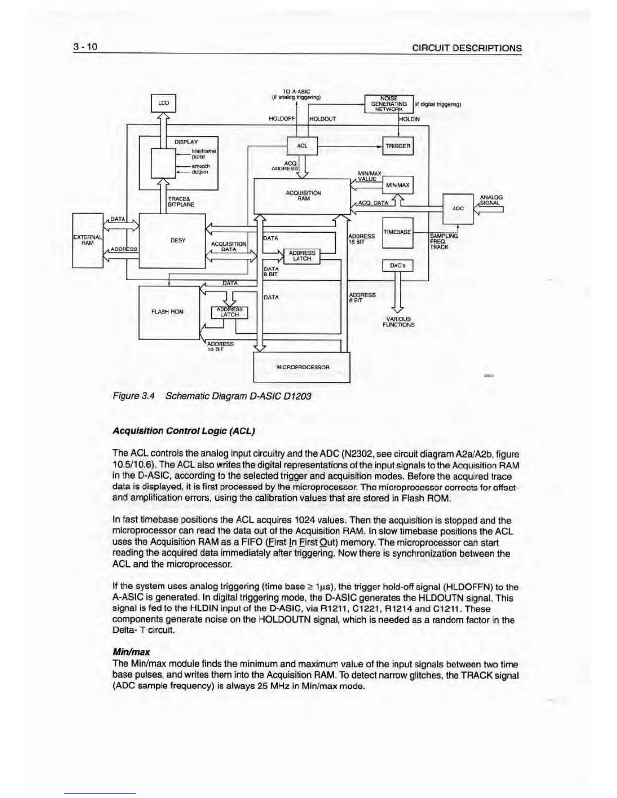
Figure 3.4 Schematic
Diagram D-ASIC D1203
Acquisition
Control Logic (ACL)
The ACL controls the analog input circuitry
and the ADC (N2302, see circuit diagram
A2a/A2b, figure
1
0.5/1 0.6). The ACL also writes the digital representations
of the input signals to the Acquisition RAM
in the 0-ASIC, according to the
selected trigger and acquisition
modes. Before the acquired trace
data is displayed, It is first processed
by the microprocessor. The microprocessor corrects
for offset-
and ampitfication errors, using the calibration
values that are stored In Flash ROM.
In fast timebase positions
the ACL acquires 1024 values.
Then the acquisition Is stopped
and
the
microprocessor
can read the data out of the AcqulSjtior\
RAM. In slow timebase positions the ACL
uses the Acquisition
RAM as a FIFO ®rs!
In
First
Qut) memory. The microprocessor can
start
reading
the acquired data Immediately after triggering.
Now there is synchronization between
the
ACL and the microprocessor.
If the system uses analog triggering (time
base ^ l^s), the trigger hold-off signal
(HLDOFFN) to the
A-ASIC is generated. In digital triggering
mode, the D-ASIC generates the HLDOUTN signal.
This
signal
1$ fed to the HLDIN input of the D-ASIC, via
R1 211, C1221, R1214 and C1 211.
These
components
generate noise on the HOLDOUTN signal,
which is needed as a random factor in the
Delta- T circuit.
Min/max
The
Mln/max module finds the minimum and maximum value
of the input signals between two time
base pulses, and writes them into the
Acquisition RAM. To detect narrow glitches, the TRACK
signal
(ADC sample frequency) is always 25 Ml-lz
in MirVmax mode.