CIRCUIT DESCRIPTIONS 3-11
Di6ptay contra/
This module reads screen data from the External RAMs
(D1
204
and D1
205)
and sends It to the LCD.
it also sends line pulses UNECL
(17
kHz)
and frame pulses FRAME (70 Hz). This screen data,
consisting of for example cursor and grid information,
Is stored In External RAMs as bltplane
information. The trace data
Is
stored
as a value
tor
every vertical line on the LCD. This data is
converted to bitplar^
data and added to the cursor and grid Information. The display control module
also makes It possible
to change the dotsize of the signal displayed and to use dot joining.
Decoding and synchronization (DESY)
The DESY section is the decoder for the D-AStC’s
internal addresses. This module also synchronises
the microprocessor with the D-ASIC's Display control
module, as botii access the same Acquisition
RAM.
DigiW to ana/og converters (DACs)
The DACs module contains
10 one-bft pulse width modulated monotonous DACs, whose resolution
ranges from five to ten bts. The
DACs are used to control level shifting, analog trigger level, LCD
contrast and the generator function (see section 3.4.7).
Externa/ RAMs
The External RAM section consists of two 32K •
d
SRAMs
(D1204 and D1206). These RAMs contain:
•
wavefonms (stored with the WAVEFORM
key)
•
frontsettings (stored with tiie SETUP key)
>
bltplane data for the LCD picture
‘
text, to be used on the display
•
data in RECORD mode
-
data in A versus B modo (A»
t ^
)
•
bltplane data used while making a printout
of
the screen
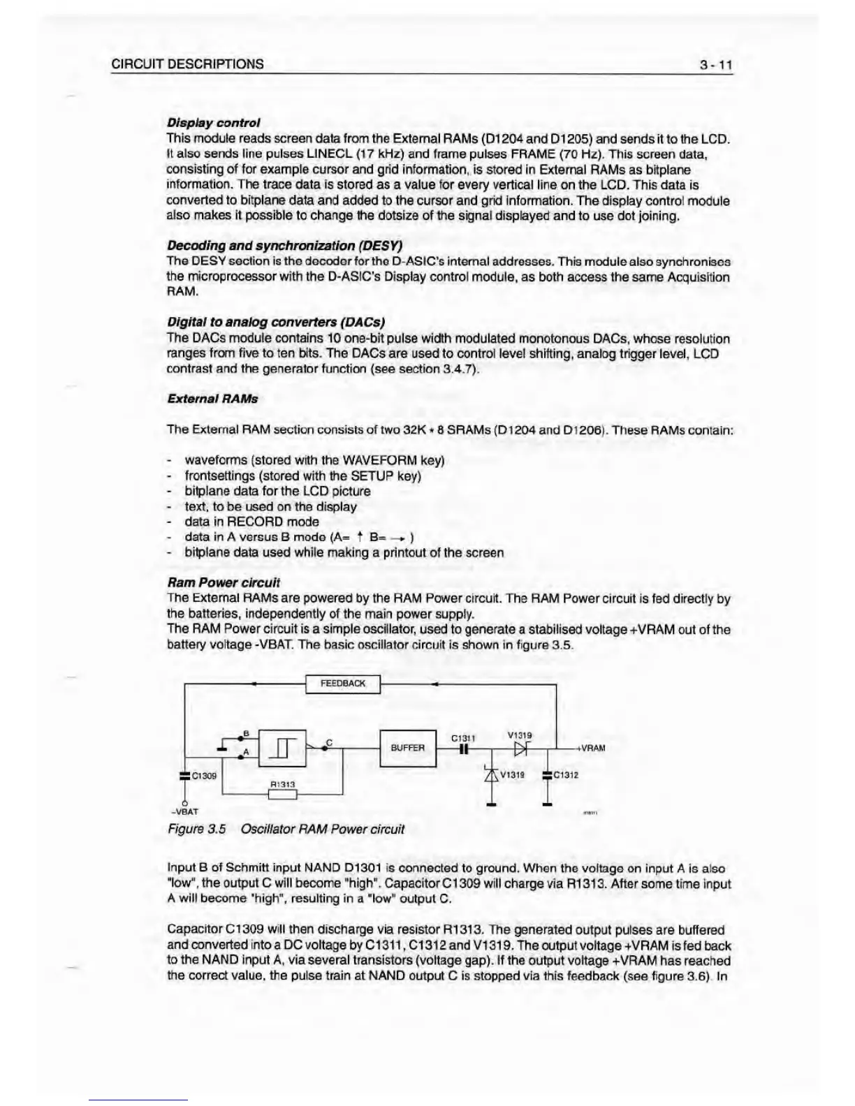
Ram Power circuit
The External
RAMs are powered by the RAM Power circuit. The RAM Power circuit
is fed directly by
the batteries, independently
of the main power supply.
The RAM
Power
circuit is a simple oscillator, used
to
generate
a stabilised voltage -fVRAM out of the
battery voltage -VBAT.
The basic oscillator circuit is ^own in figure 3.5.
-VBAT
Figure
3.5 Osc/7/afor RAM Power circuit
Input B of Schmitt input NAND D1301 is
connected to ground. When the voltage on input
A is
also
low", the ou5>ut C will become "high". Capacitor
Cl 309
will
charge via R1313. After some time
input
A will become 'high", resulting in
a
"low"
output C.
C^>acitorCi309 will
then discharge via resistor R1313. The generated
output pulses are buffered
and converted i
nto a DC voltage by C1 31
1 ,
C1 31 2 and V1 31 9. Th
e outp
ut voltag
e +VRAM Is fed back
to the NAND input
A, via several transistors (voltage gap). If the output voltage
-fVRAM has reached
the correct value, trie pulse train at NAND
output C
is
stopped via this feedback (see figure 3.6). In