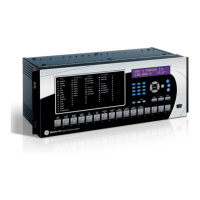
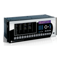
B-52 F60 Feeder Protection System GE Multilin
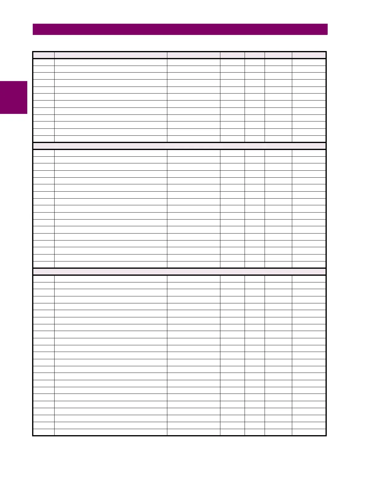
B.4 MEMORY MAPPING APPENDIX B
B
900F FlexElement 1 Pickup Delay 0 to 65.535 s 0.001 F001 0
9010 FlexElement 1 Reset Delay 0 to 65.535 s 0.001 F001 0
9011 FlexElement 1 Block 0 to 4294967295 --- 1 F300 0
9013 FlexElement 1 Target 0 to 2 --- 1 F109 0 (Self-reset)
9014 FlexElement 1 Events 0 to 1 --- 1 F102 0 (Disabled)
9015 ...Repeated for FlexElement 2
902A ...Repeated for FlexElement 3
903F ...Repeated for FlexElement 4
9054 ...Repeated for FlexElement 5
9069 ...Repeated for FlexElement 6
907E ...Repeated for FlexElement 7
9093 ...Repeated for FlexElement 8
Fault Report Settings (Read/Write Setting)
9200 Fault Report 1 Source 0 to 5 --- 1 F167 0 (SRC 1)
9201 Fault Report 1 Trigger 0 to 4294967295 --- 1 F300 0
9203 Fault Report 1 Z1 Magnitude 0.01 to 250 ohms 0.01 F001 300
9204 Fault Report 1 Z1 Angle 25 to 90 degrees 1 F001 75
9205 Fault Report 1 Z0 Magnitude 0.01 to 650 ohms 0.01 F001 900
9206 Fault Report 1 Z0 Angle 25 to 90 degrees 1 F001 75
9207 Fault Report 1 Line Length Units 0 to 1 --- 1 F147 0 (km)
9208 Fault Report 1 Line Length 0 to 2000 --- 0.1 F001 1000
9209 Fault Report 1 VT Substitution 0 to 2 --- 1 F270 0 (None)
920A Fault Report 1 System Z0 Magnitude 0.01 to 650.00 ohms 0.01 F001 200
9208 Fault Report 1 System Z0 Angle 25 to 90 degrees 1 F001 75
920C Fault REM1-TAP Z1 Magnitude 0.01 to 250 ohms 0.01 F001 300
920D Fault REM1-TAP Z1 Angle 25 to 90 degrees 1 F001 75
920E Fault REM1-TAP Length 0 to 2000 --- 0.1 F001 1000
920F Fault REM2-TAP Z1 Magnitude 0.01 to 250 ohms 0.01 F001 300
9210 Fault REM2-TAP Z1 Angle 25 to 90 degrees 1 F001 75
9211 Fault REM2-TAP Length 0 to 2000 --- 0.1 F001 1000
DCmA Outputs (Read/Write Setting) (24 modules)
9360 DCmA Output 1 Source 0 to 65535 --- 1 F600 0
9361 DCmA Output 1 Range 0 to 2 --- 1 F522 0 (–1 to 1 mA)
9362 DCmA Output 1 Minimum –90 to 90 pu 0.001 F004 0
9364 DCmA Output 1 Maximum –90 to 90 pu 0.001 F004 1000
9366 ...Repeated for DCmA Output 2
936C ...Repeated for DCmA Output 3
9372 ...Repeated for DCmA Output 4
9378 ...Repeated for DCmA Output 5
937E ...Repeated for DCmA Output 6
9384 ...Repeated for DCmA Output 7
938A ...Repeated for DCmA Output 8
9390 ...Repeated for DCmA Output 9
9396 ...Repeated for DCmA Output 10
939C ...Repeated for DCmA Output 11
93A2 ...Repeated for DCmA Output 12
93A8 ...Repeated for DCmA Output 13
93AE ...Repeated for DCmA Output 14
93B4 ...Repeated for DCmA Output 15
93BA ...Repeated for DCmA Output 16
93C0 ...Repeated for DCmA Output 17
93C6 ...Repeated for DCmA Output 18
93CC ...Repeated for DCmA Output 19
93D2 ...Repeated for DCmA Output 20
Table B–10: MODBUS MEMORY MAP (Sheet 44 of 70)
ADDR REGISTER NAME RANGE UNITS STEP FORMAT DEFAULT