37
Chapter 4. LVCMOS Communication Protocol
4.1 Thermal Camera Module Video Output
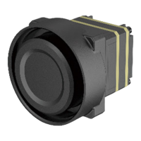
The thermal camera module has two different shapes with different video data output, as shown in Figure
4-1.
Figure4-1 Thermal Camera Module LVCMOS Video Output
Note:
All the data stream for HM-TM36-LG/D BT.656 output and HM-TM36-LG/S are processed by ISP
algorithm.
In YUV + RAW output, the data stream does not support the menu, mirror, reticle and zoom. In YUV
output, the stream only supports the palette.
4.2 HM-TM36-LG/D Output
The HM-TM36-LG/D thermal camera module contains a 16 bit LVCMOS digital video output. The video
output can switch between BT.656 internal synchronization and YUV + RAW external synchronization.
The frequency of pixel clock is 27 MHz for BT.656 output, and for YUV + RAW output, the frequency of
pixel clock is 54 MHz. For the detailed switch method, refer to 3.8.9 Data Switching or operate through the
client software.
4.2.1 BT.656
For the HM-TM36-LG/D thermal camera module with the BT.656 data output, the CVBS output follows
ITU-RBT.656 (PAL, 720 × 576) video interface standard and the frequency of pixel clock is 27 MHz.
A field of video output consists of four sections.
 Loading...