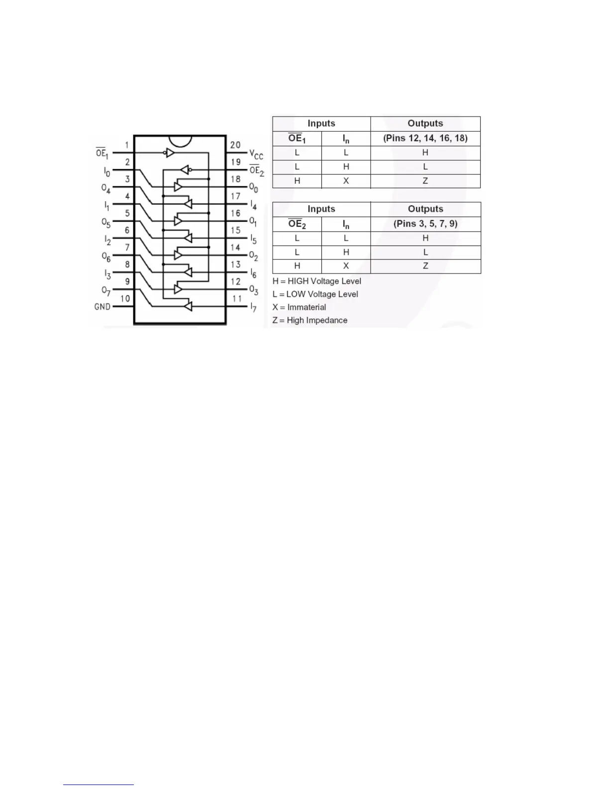
15.11.4. Pinning
15.12. 74LCX245
15.12.1. General Description
The LCX245 contains eight non-inverting bidirectional buffers with 3-STATE outputs and
is intended for bus oriented applications. The device is designed for low voltage (2.5V
and 3.3V) VCC applications with capability of interfacing to a 5V signal environment.
The T/R input determines the direction of data flow through the device. The OE input
disables both the A and B ports by placing them in a high impedance state.
The LCX245 is fabricated with an advanced CMOS technology to achieve high speed
operation while maintaining CMOS low power dissipation.
15.12.2. Features
x 5V tolerant inputs and outputs
x 2.3V to 3.6V VCC specifications provided
x 7.0ns tPDmax. (VCC=3.3V), 10μA ICCmax.
x Power down high impedance inputs and outputs
x Supports live insertion/withdrawal
x ±24mA output drive (VCC=3.0V)
x Implements patented noise/EMI reduction circuitry
x Latch-up performance exceeds 500mA
x ESD performance: Human body model>2000V, Machine model>200V
x Leadless DQFN package