8.2. Features
x 3.3V for VDD and 2.5V for VDDQ power supply
x All inputs and outputs are compatible with SSTL_2 interface
x JEDEC standard 400mil 66pin TSOP-II with 0.65mm pin pitch
x Fully differential clock inputs (CK, /CK) operation
x Double data rate interface
x Source synchronous - data transaction aligned to bidirectional data strobe (DQS)
x x16 device has 2 bytewide data strobes (LDQS, UDQS) per each x8 I/O
x Data outputs on DQS edges when read (edged DQ) Data inputs on DQS centers
when write (centered DQ)
x Data(DQ) and Write masks(DM) latched on the both rising and falling edges of
the data strobe
x All addresses and control inputs except Data, Data strobes and Data masks
latched on the rising edges of the clock
x Write mask byte controls by LDM and UDM
x Programmable /CAS latency 3 / 4 supported
x Programmable Burst Length 2 / 4 / 8 with both sequential and interleave mode
x Internal 4 bank operations with single pulsed /RAS
x tRAS Lock-Out function supported
x Auto refresh and self refresh supported
x 4096 refresh cycles / 32ms
x Full, Half and Matched Impedance(Weak) strength driver option controlled by
EMRS
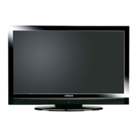
8.3. Absolute Maximum Ratings