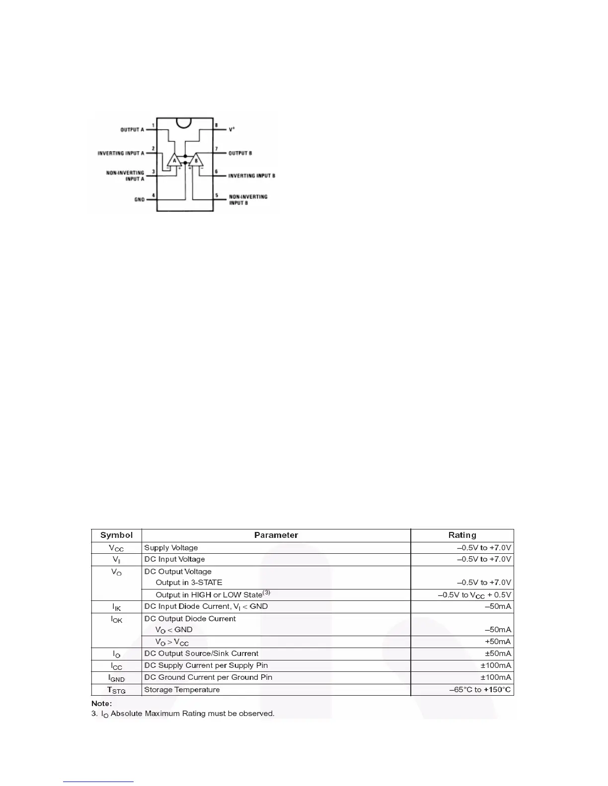
15.10.4. Pinning
15.11. 74LCX244
15.11.1. General Description
The LCX244 contains eight non-inverting buffers with 3-STATE outputs. The device may
be employed as a memory address driver, clock driver and bus-oriented
transmitter/receiver. The LCX244 is designed for low voltage (2.5V or 3.3V) VCC
applications with capability of interfacing to a 5V signal environment. The LCX244 is
fabricated with an advanced CMOS technology to achieve high speed operation while
maintaining CMOS low power dissipation.
15.11.2. Features
x 5V tolerant inputs and outputs
x 2.3V to 3.6V VCC specifications provided
x 6.5ns Tpd max. (VCC=3.3V), 10μA ICCmax.
x Power down high impedance inputs and outputs
x Supports live insertion/withdrawal
x ±24mA output drive (VCC=3.0V)
x Implements patented noise/EMI reduction circuitry
x Latch-up performance exceeds 500mA
x ESD performance:Human body model>2000V, Machine model>200V
x Leadless DQFN package
15.11.3. Absolute Maximum Ratings