15.15. MT48LC4M16A2TG8E
15.15.1. General Description
The 64Mb SDRAM is a high-speed CMOS, dynamic random-access memory containing
67,108,864 bits. It is internally configured as a quad-bank DRAM with a synchronous
interface (all signals are registered on the positive edge of the clock signal, CLK). Each
of the x4’s 16,777,216-bit banks is organized as 4,096 rows by 1,024 columns by 4 bits.
Each of the x8’s 16,777,216-bit banks is organized as 4,096 rows by 512 columns by 8
bits. Each of the x16’s 16,777,216-bit banks is organized as 4,096 rows by 256 columns
by 16 bits. Read and write accesses to the SDRAM are burst oriented; accesses start at
a selected location and continue for a programmed number of locations in a
programmed sequence. Accesses begin with the registration of an ACTIVE command,
which is then ollowed by a READ or WRITE command. The address bits registered
coincident with the ACTIVE command are used to select the bank and row to be
accessed (BA0, BA1 select the bank; A0-A11 select the row).
15.15.2. Features
x PC66-, PC100- and PC133-compliant
x 143 MHz, graphical 4 Meg x 16 option
x Fully synchronous; all signals registered on positive edge of system clock
x Internal pipelined operation; column address can be changed every clock cycle
x Internal banks for hiding row access/precharge
x Programmable burst lengths: 1, 2, 4, 8 or full page
x Auto Precharge, includes CONCURRENT AUTO PRECHARGE, and AutO
Refresh Modes
x Self Refresh Modes: standard and low power
x 64ms, 4,096-cycle refresh
x LVTTL-compatible inputs and outputs
x Single +3.3V ±0.3V power supply
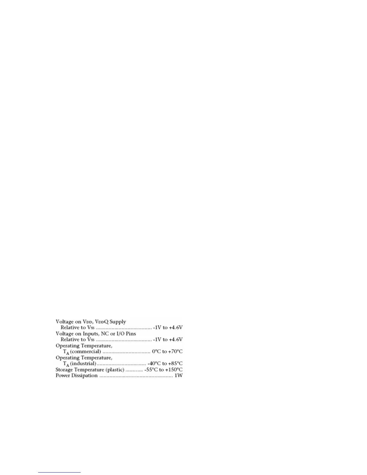
15.15.3. Absolute Maximum Ratings