Rev. 1.50 10 August 28, 2017 Rev. 1.50 11 August 28, 2017
HT66F0175/HT66F0185
A/D Flash MCU with EEPROM
HT66F0175/HT66F0185
A/D Flash MCU with EEPROM
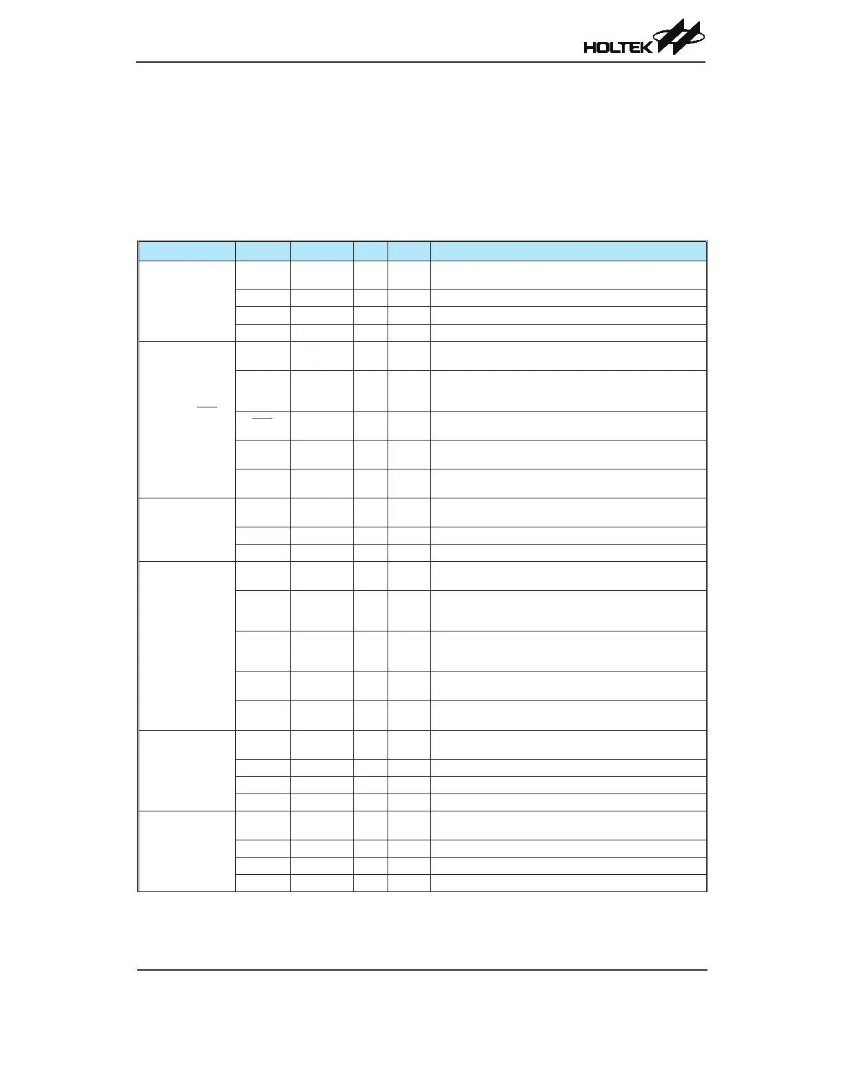
Pin Descriptions
Withtheexceptionofthepowerpins,allpinsonthesedevicescanbereferencedbytheirPortname,
e.g.PA0,PA1etc,whichrefertothedigitalI/Ofunctionofthepins.HoweverthesePortpinsare
alsosharedwithotherfunctionsuchastheAnalogtoDigitalConverter,TimerModulepins,etc.
Thefunctionofeachpinislistedinthefollowingtable,howeverthedetailsbehindhoweachpinis
congurediscontainedinothersectionsofthedatasheet.
HT66F0175
Pad Name Function OPT I/T O/T Description
PA0/TP0/ICPDA/
OCDSDA
PA0
PAWU
PAPU
ST CMOS
General purpose I/O. Register enabled pull-up and
wake-up.
TP0 TMPC ST CMOS TM0 input/output
ICPDA — ST CMOS ICP Data/Address pin
OCDSDA — ST CMOS OCDS Data/Address pin, for EV chip only.
PA1/[SDO]/SCS/
SSEG2/SCOM2
PA1
PAWU
PAPU
ST CMOS
General purpose I/O. Register enabled pull-up and
wake-up.
[SDO]
SLCDC0
SIMC0
IFS
— CMOS SPI data output
SCS
SLCDC0
SIMC0 IFS
ST CMOS SPI slave select
SSEG2
SLCDC0
SLCDC1
— SSEG Software controlled LCD segment output
SCOM2
SLCDC0
SLCDC1
— SCOM Software controlled LCD common output
PA2/ICPCK/
OCDSCK
PA2
PAWU
PAPU
ST CMOS
General purpose I/O. Register enabled pull-up and
wake-up.
ICPCK — ST CMOS ICP Clock pin
OCDSCK — ST — OCDS Clock pin, for EV chip only.
PA3/[SDI/SDA]/
SSEG3/SCOM3
PA3
PAWU
PAPU
ST CMOS
General purpose I/O. Register enabled pull-up and
wake-up.
[SDI]
SLCDC0
SIMC0
IFS
ST — SPI data input
[SDA]
SLCDC0
SIMC0
IFS
ST NMOS I
2
C address/data line
SSEG3
SLCDC0
SLCDC1
— SSEG Software controlled LCD segment output
SCOM3
SLCDC0
SLCDC1
— SCOM Software controlled LCD common output
PA4/TCK1/
SSEG13/AN3
PA4
PAWU
PAPU
ST CMOS
General purpose I/O. Register enabled pull-up and
wake-up.
TCK1 TM1C0 ST — TM1 input
SSEG13 SLCDC2 — SSEG Software controlled LCD segment output
AN3 ACERL AN — A/D Converter analog input
PA5/SSEG10/
AN4/VREFI
PA5
PAWU
PAPU
ST CMOS
General purpose I/O. Register enabled pull-up and
wake-up.
SSEG10 SLCDC2 — SSEG Software controlled LCD segment output
AN4 ACERL AN — A/D Converter analog input
VREFI SADC2 AN — A/D Converter PGA voltage input