Rev. 1.50 28 August 28, 2017 Rev. 1.50 29 August 28, 2017
HT66F0175/HT66F0185
A/D Flash MCU with EEPROM
HT66F0175/HT66F0185
A/D Flash MCU with EEPROM
Table Read Program Example
tempreg1 db ? ; temporary register #1
tempreg2 db ? ; temporary register #2
:
mov a,06h ; initialise low table pointer - note that this address is referenced
mov tblp,a ; to the last page or the page that tbhp pointed
mov a,0fh ; initialise high table pointer
mov tbhp,a
:
tabrd tempreg1 ; transfers value in table referenced by table pointer data at program
; memory address “0F06H” transferred to tempreg1 and TBLH
dec tblp ; reduce value of table pointer by one
tabrd tempreg2 ; transfers value in table referenced by table pointer data at program
; memory address “0F05H” transferred to tempreg2 and TBLH in this
; example the data “1AH” is transferred to tempreg1 and data “0FH” to
; register tempreg2
:
org 0F00h ; sets initial address of program memory
dc 00Ah, 00Bh, 00Ch, 00Dh, 00Eh, 00Fh, 01Ah, 01Bh
:
In Circuit Programming – ICP
TheprovisionofFlashtypeProgramMemoryprovidestheuserwithameansofconvenientand
easyupgradesandmodicationstotheirprogramsonthesamedevice.
Asanadditionalconvenience,Holtekhasprovidedameansofprogrammingthemicrocontrollerin-
circuitusinga4-pininterface.Thisprovidesmanufacturerswiththepossibilityofmanufacturing
theircircuitboardscompletewithaprogrammedorun-programmedmicrocontroller,andthen
programmingorupgradingtheprogramatalaterstage.Thisenablesproductmanufacturerstoeasily
keeptheirmanufacturedproductssuppliedwiththelatestprogramreleaseswithoutremovalandre-
insertionofthedevice.
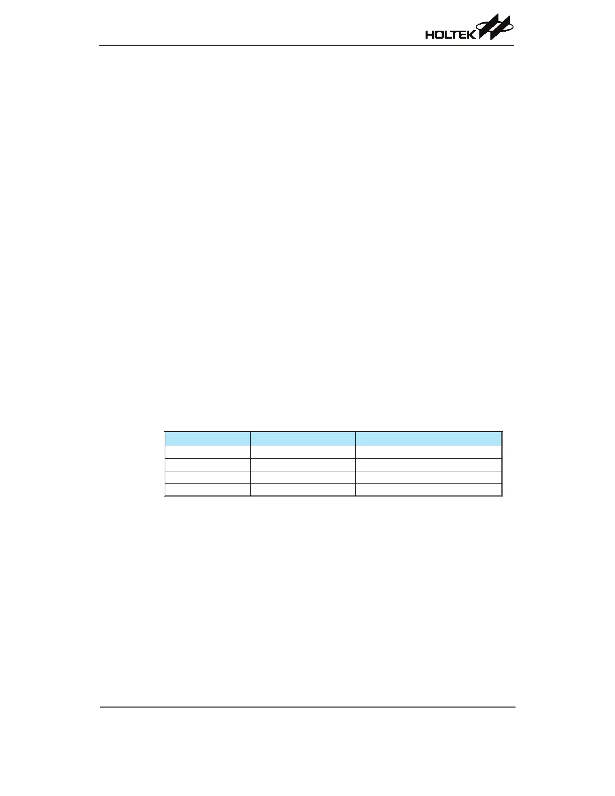
Holtek Writer Pins MCU Programming Pins Pin Description
ICPDA PA0 Programming Serial Data/Address
ICPCK PA2 Programming Clock
VDD VDD Power Supply
VSS VSS Ground
TheProgramMemoryandEEPROMdatamemorycanbeprogrammedseriallyin-circuitusingthis
4-wireinterface.Dataisdownloadedanduploadedseriallyonasinglepinwithanadditionalline
fortheclock.Twoadditionallinesarerequiredforthepowersupply.Thetechnicaldetailsregarding
thein-circuitprogrammingofthedevicearebeyondthescopeofthisdocumentandwillbesupplied
insupplementaryliterature.
Duringtheprogrammingprocess,theusermusttakecareoftheICPDAandICPCKpinsfordata
andclockprogrammingpurposestoensurethatnootheroutputsareconnectedtothesetwopins.