Rev. 1.50 124 August 28, 2017 Rev. 1.50 125 August 28, 2017
HT66F0175/HT66F0185
A/D Flash MCU with EEPROM
HT66F0175/HT66F0185
A/D Flash MCU with EEPROM
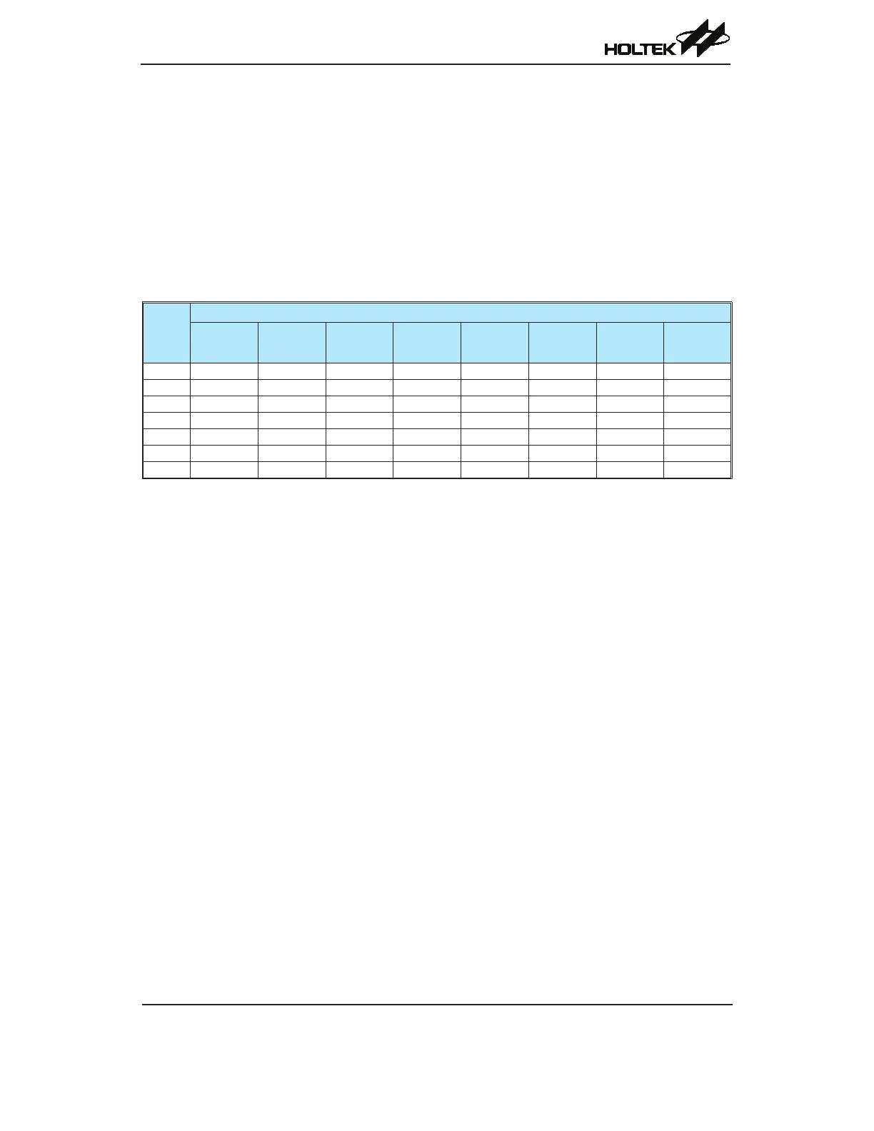
TheclocksourcefortheA/Dconverter,whichoriginatesfromthesystemclockf
SYS
,canbechosen
tobeeitherf
SYS
orasubdividedversionoff
SYS
.Thedivisionratiovalueisdeterminedbythe
SACKS2~SACKS0bitsintheSADC1register.AlthoughtheA/Dclocksourceisdeterminedbythe
systemclockf
SYS
andbybitsSACKS2~SACKS0,therearesomelimitationsonthemaximumA/D
clocksourcespeedthatcanbeselected.AstherecommendedrangeofpermissibleA/Dclockperiod,
t
ADCK
,isfrom0.5μsto10μs,caremustbetakenforsystemclockfrequencies.Forexample,asthe
systemclockoperatesatafrequencyof8MHz,theSACKS2~SACKS0bitsshouldnotbesetto000,
001or111.DoingsowillgiveA/DclockperiodsthatarelessthantheminimumA/Dclockperiod
whichmayresultininaccurateA/Dconversionvalues.Refertothefollowingtableforexamples,
wherevaluesmarkedwithanasterisk*showwhere,dependinguponthedevices,specialcaremust
betaken,asthevaluesmaybelessthanthespeciedminimumA/DClockPeriod.
f
SYS
A/D Clock Period (t
ADCK
)
SACKS[2:0]
= 000
(f
SYS
)
SACKS[2:0]
= 001
(f
SYS
/2)
SACKS[2:0]
= 010
(f
SYS
/4)
SACKS[2:0]
= 011
(f
SYS
/8)
SACKS[2:0]
= 100
(f
SYS
/16)
SACKS[2:0]
= 101
(f
SYS
/32)
SACKS[2:0]
= 110
(f
SYS
/64)
SACKS[2:0]
= 111
(f
SYS
/128)
1 MHz 1μs 2μs 4μs 8μs 16μs * 32μs * 64μs * 128μs *
2 MHz 500ns 1μs 2μs 4μs 8μs 16μs * 32μs * 64μs *
4 MHz 250ns * 500ns 1μs 2μs 4μs 8μs 16μs * 32μs *
8 MHz 125ns * 250ns * 500ns 1μs 2μs 4μs 8μs 16μs *
12 MHz 83ns * 167ns * 333ns * 667ns 1.33μs 2.67μs 5.33μs 10.67μs *
16 MHz 62.5ns * 125ns * 250ns * 500ns 1μs 2μs 4μs 8μs
20 MHz 50ns * 100ns * 200ns * 400ns * 800ns 1.6μs 3.2μs 6.4μs
A/D Clock Period Examples
Controllingthepoweron/offfunctionoftheA/Dconvertercircuitryisimplementedusingthe
ADCENbitintheSADC0register.ThisbitmustbesethightopowerontheA/Dconverter.When
theADCENbitissethightopowerontheA/Dconverterinternalcircuitry,acertaindelay,as
indicatedinthetimingdiagram,mustbeallowedbeforeanA/Dconversionisinitiated.Evenif
nopinsareselectedforuseasA/Dinputs,iftheADCENbitishigh,thensomepowerwillstillbe
consumed.InpowerconsciousapplicationsitisthereforerecommendedthattheADCENissetlow
toreducepowerconsumptionwhentheA/Dconverterfunctionisnotbeingused.
Conversion Rate and Timing Diagram
AcompleteA/Dconversioncontainstwoparts,datasamplinganddataconversion.Thedata
samplingwhichisdenedast
ADS
takes4A/Dclockcyclesandthedataconversiontakes12A/D
clockcycles.Thereforeatotalof16A/DclockcyclesforanA/Dconversionwhichisdenedast
ADC
arenecessary.
MaximumsingleA/Dconversionrate=A/Dclockperiod/16(1)
Theaccompanyingdiagramshowsgraphicallythevariousstagesinvolvedinananalogtodigital
conversionprocessanditsassociatedtiming.AfteranA/Dconversionprocesshasbeeninitiated
bytheapplicationprogram,themicrocontrollerinternalhardwarewillbegintocarryoutthe
conversion,duringwhichtimetheprogramcancontinuewithotherfunctions.Thetimetakenforthe
A/Dconversionis16t
ADCK
clockcycleswheret
ADCK
isequaltotheA/Dclockperiod.