Rev. 1.50 116 August 28, 2017 Rev. 1.50 117 August 28, 2017
HT66F0175/HT66F0185
A/D Flash MCU with EEPROM
HT66F0175/HT66F0185
A/D Flash MCU with EEPROM
Analog to Digital Converter
Theneedtointerfacetorealworldanalogsignalsisacommonrequirementformanyelectronic
systems.However,toproperlyprocessthesesignalsbyamicrocontroller,theymustfirstbe
convertedintodigitalsignalsbyA/Dconverters.ByintegratingtheA/Dconversionelectronic
circuitryintothemicrocontroller,theneedforexternalcomponentsisreducedsignicantlywiththe
correspondingfollow-onbenetsoflowercostsandreducedcomponentspacerequirements.
A/D Overview
Thesedevicescontainamulti-channelanalogtodigitalconverterwhichcandirectlyinterfaceto
externalanalogsignals,suchasthatfromsensorsorothercontrolsignalsandconvertthesesignals
directlyintoa12-bitdigitalvalue.Italsocanconverttheinternalsignals,suchastheBandgap
referencevoltage,intoa12-bitdigitalvalue.Theexternalorinternalanalogsignaltobeconvertedis
determinedbytheSAINS2~SAINS0bitstogetherwiththeSACS2~SACS0bits.Notethatwhenthe
externalandinternalanalogsignalsaresimultaneouslyselectedtobeconverted,theinternalanalog
signalwillhavethepriority.Inthemeantimetheexternalanalogsignalwilltemporarilybeswitched
offuntiltheinternalanalogsignalisdeselected.MoredetailedinformationabouttheA/Dinput
signalisdescribedinthe“A/DConverterControlRegisters”and“A/DConverterInputSignal”
sectionsrespectively.
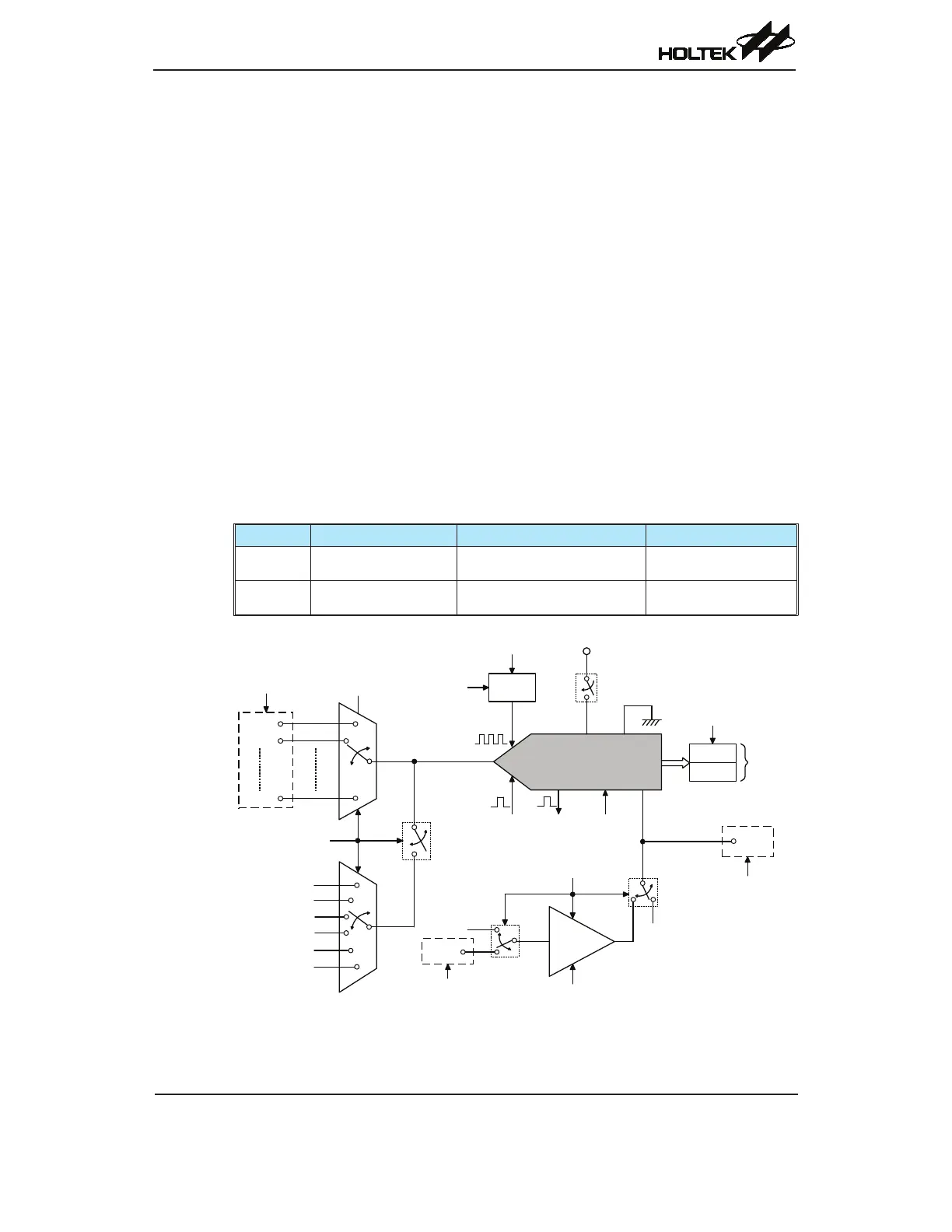
TheaccompanyingblockdiagramshowstheinternalstructureoftheA/Dconvertertogetherwithits
associatedregisters.
Device External Input Channel Internal Analog Signals A/D Signal Select Bits
HT66F0175 AN0~AN7 V
DD
, V
DD
/2, V
DD
/4, V
R
, V
R
/2, V
R
/4
SAINS2~SAINS0;
SACS2~SACS0
HT66F0185 AN0~AN7 V
DD
, V
DD
/2, V
DD
/4, V
R
, V
R
/2, V
R
/4
SAINS2~SAINS0;
SACS2~SACS0
ACE7~ACE0
SACS2~SACS0
SAINS2~SAINS0
A/D Converter
START ADBZ ADCEN
V
SS
A/D Clock
÷2
N
(N=0~7)
f
SYS
SACKS2~
SACKS0
V
DD
ADCEN
SADOL
SADOH
AN0
AN1
AN7
A/D Reference Voltage
A/D Data
Registers
V
DD
V
DD
/2
V
DD
/4
V
R
V
R
/2
V
R
/4
ADRFS
PGA
V
RI
V
REFI
V
BG
(Gain=1~4)
SAVRS3~SAVRS0
ADPGAEN
V
REF
V
R
V
DD
VREFPS
VREFIPS
A/D Converter Structure