Rev. 1.50 126 August 28, 2017 Rev. 1.50 127 August 28, 2017
HT66F0175/HT66F0185
A/D Flash MCU with EEPROM
HT66F0175/HT66F0185
A/D Flash MCU with EEPROM
ADCEN
START
ADBZ
SACS[2:0]
off on off on
t
ON2ST
t
ADS
A/D sampling time
t
ADS
A/D sampling time
Start of A/D conversion Start of A/D conversion Start of A/D conversion
End of A/D
conversion
End of A/D
conversion
t
ADC
A/D conversion time
t
ADC
A/D conversion time
t
ADC
A/D conversion time
011B 010B 000B 001B
A/D channel
switch
(SAINS =000B)
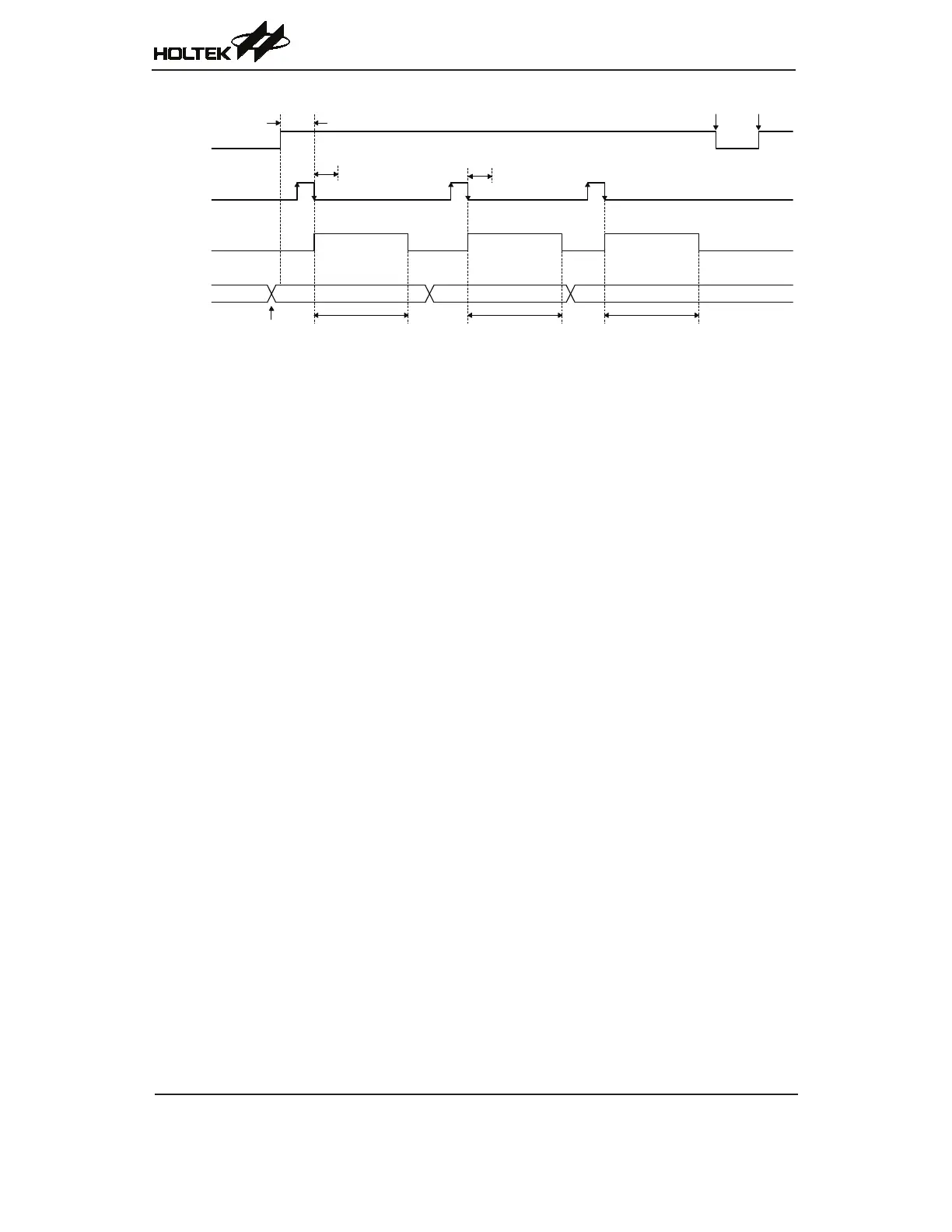
A/D Conversion Timing
Summary of A/D Conversion Steps
ThefollowingsummarisestheindividualstepsthatshouldbeexecutedinordertoimplementanA/D
conversionprocess.
Step 1
SelecttherequiredA/DconversionclockbyproperlyprogrammingtheSACKS2~SACKS0bitsin
theSADC1register.
Step 2
EnabletheA/DconverterbysettingtheADCENbitintheSADC0registerto1.
Step 3
SelectwhichsignalistobeconnectedtotheinternalA/Dconverterbycorrectlyconguringthe
SAINS2~SAINS0bits
Selecttheexternalchannelinputtobeconverted,gotoStep4.
Selecttheinternalanalogsignaltobeconverted,gotoStep5.
Step 4
IftheA/DinputsignalcomesfromtheexternalchannelinputselectingbyconguringtheSAINS
biteld,thecorrespondingpinsshouldrstbeconguredasA/Dinputfunctionbyconguringthe
relevantpin-sharedfunctioncontrolbits.Thedesiredanalogchannelthenshouldbeselectedby
conguringtheSACSbiteld.Afterthisstep,gotoStep6.
Step 5
IftheA/Dinputsignalisselectedtocomefromtheinternalanalogsignal,theSAINSbitfield
shouldbeproperlyconguredandthentheexternalchannelinputwillautomaticallybedisconnected
regardlessoftheSACSbiteldvalue.Afterthisstep,gotoStep6.
Step 6
SelectthereferencevoltgagesourcebyconguringtheSAVRS3~SAVRS0bits.
Step 7
SelecttheA/DconverteroutputdataformatbyconguringtheADRFSbit.