Rev. 1.50 126 August 28, 2017 Rev. 1.50 127 August 28, 2017
HT66F0175/HT66F0185
A/D Flash MCU with EEPROM
HT66F0175/HT66F0185
A/D Flash MCU with EEPROM
Step 8
IfA/Dconversioninterruptisused,theinterruptcontrolregistersmustbecorrectlyconfigured
toensuretheA/Dinterruptfunctionisactive.Themasterinterruptbontrolbit,EMI,andtheA/D
conversioninterruptcontrolbit,ADE,mustbothbesethighinadvance.
Step 9
TheA/DconversionprocedurecannowbeinitializedbysettingtheSTARTbitfromlowtohighand
thenlowagain.
Step 10
IfA/Dconversionisinprogress,theADBZagwillbesethigh.AftertheA/Dconversionprocess
iscomplete,theADBZagwillgolowandthentheoutputdatacanbereadfromSADOHand
SADOLregisters.
Note:Whencheckingfortheendoftheconversionprocess,ifthemethodofpollingtheADBZbitinthe
SADC0registerisused,theinterruptenablestepabovecanbeomitted.
Programming Considerations
DuringmicrocontrolleroperationswheretheA/Dconverterisnotbeingused,theA/Dinternal
circuitrycanbeswitchedofftoreducepowerconsumption,bysettingbitADCENlowinthe
SADC0register.Whenthishappens,theinternalA/Dconvertercircuitswillnotconsumepower
irrespectiveofwhatanalogvoltageisappliedtotheirinputlines.IftheA/Dconverterinputlinesare
usedasnormalI/Os,thencaremustbetakenasiftheinputvoltageisnotatavalidlogiclevel,then
thismayleadtosomeincreaseinpowerconsumption.
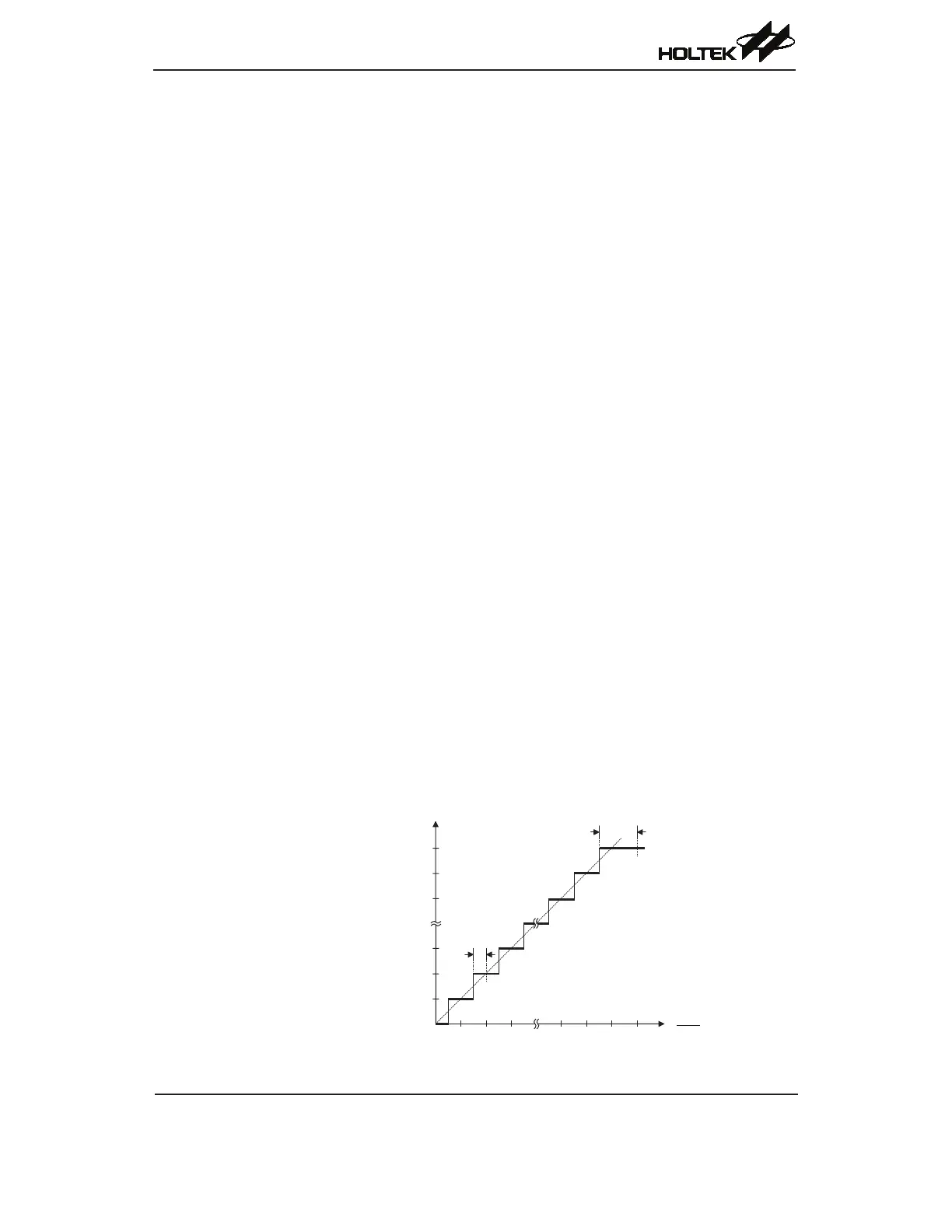
A/D Transfer Function
Asthedevicescontaina12-bitA/Dconverter,itsfull-scaleconverteddigitisedvalueisequalto
FFFH.Sincethefull-scaleanaloginputvalueisequaltotheV
REF
voltage,thisgivesasinglebit
analoginputvalueofV
REF
dividedby4096.
1LSB=V
REF
÷4096
TheA/DConverterinputvoltagevaluecanbecalculatedusingthefollowingequation:
A/Dinputvoltage=A/Doutputdigitalvalue×V
REF
÷4096
Thediagramshowstheidealtransferfunctionbetweentheanaloginputvalueandthedigitised
outputvaluefortheA/Dconverter.Exceptforthedigitisedzerovalue,thesubsequentdigitised
valueswillchangeatapoint0.5LSBbelowwheretheywouldchangewithouttheoffset,andthe
lastfullscaledigitisedvaluewillchangeatapoint1.5LSBbelowtheV
REF
level.
Ideal A/D Transfer Function