Rev. 1.50 30 August 28, 2017 Rev. 1.50 31 August 28, 2017
HT66F0175/HT66F0185
A/D Flash MCU with EEPROM
HT66F0175/HT66F0185
A/D Flash MCU with EEPROM
Data Memory
TheDataMemoryisan8-bitwideRAMinternalmemoryandisthelocationwheretemporary
informationisstored.
Structure
Dividedintotwobanks,therstoftheseisanareaofRAM,knownastheSpecialFunctionData
Memory.Herearelocatedregisterswhicharenecessaryforcorrectoperationofthedevice.Many
oftheseregisterscanbereadfromandwrittentodirectlyunderprogramcontrol,however,some
remainprotectedfromusermanipulation.ThesecondareaofDataMemoryisknownastheGeneral
PurposeDataMemory,whichisreservedforgeneralpurposeuse.Alllocationswithinthisareaare
readandwriteaccessibleunderprogramcontrol.
TheoverallDataMemoryissubdividedintotwobanks.TheSpecialPurposeDataMemoryregisters
areaccessibleinallbanks,withtheexceptionoftheEECregisterataddress40H,whichisonly
accessibleinBank1.SwitchingbetweenthedifferentDataMemorybanksisachievedbysettingthe
BankPointertothecorrectvalue.ThestartaddressoftheDataMemoryforthedeviceistheaddress
00H.
TheaddressrangeoftheSpecialPurposeDataMemoryforthedeviceisfrom00Hto7FHwhilethe
addressrangeoftheGeneralPurposeDataMemoryisfrom80HtoFFH.
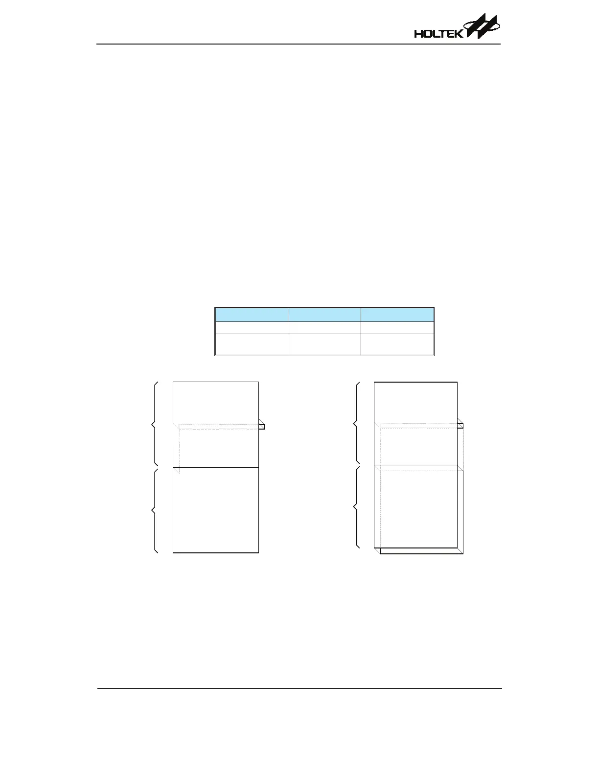
Device Capacity Banks
HT66F0175 128 × 8 0: 80H~FFH
HT66F0185 256 × 8
0: 80H~FFH
1: 80H~FFH
Data Memory Summary
00H
7FH
80H
FFH
Special
Purpose Data
Memory
General
Purpose Data
Memory
Bank 0
40H: EEC
HT66F0175
(Bank 1)
00H
7FH
80H
FFH
Special
Purpose Data
Memory
General
Purpose Data
Memory
Bank 0
Bank 1
40H:EEC
(Bank 1)
HT66F0185
Data Memory Structure