Rev. 1.50 30 August 28, 2017 Rev. 1.50 31 August 28, 2017
HT66F0175/HT66F0185
A/D Flash MCU with EEPROM
HT66F0175/HT66F0185
A/D Flash MCU with EEPROM
* *
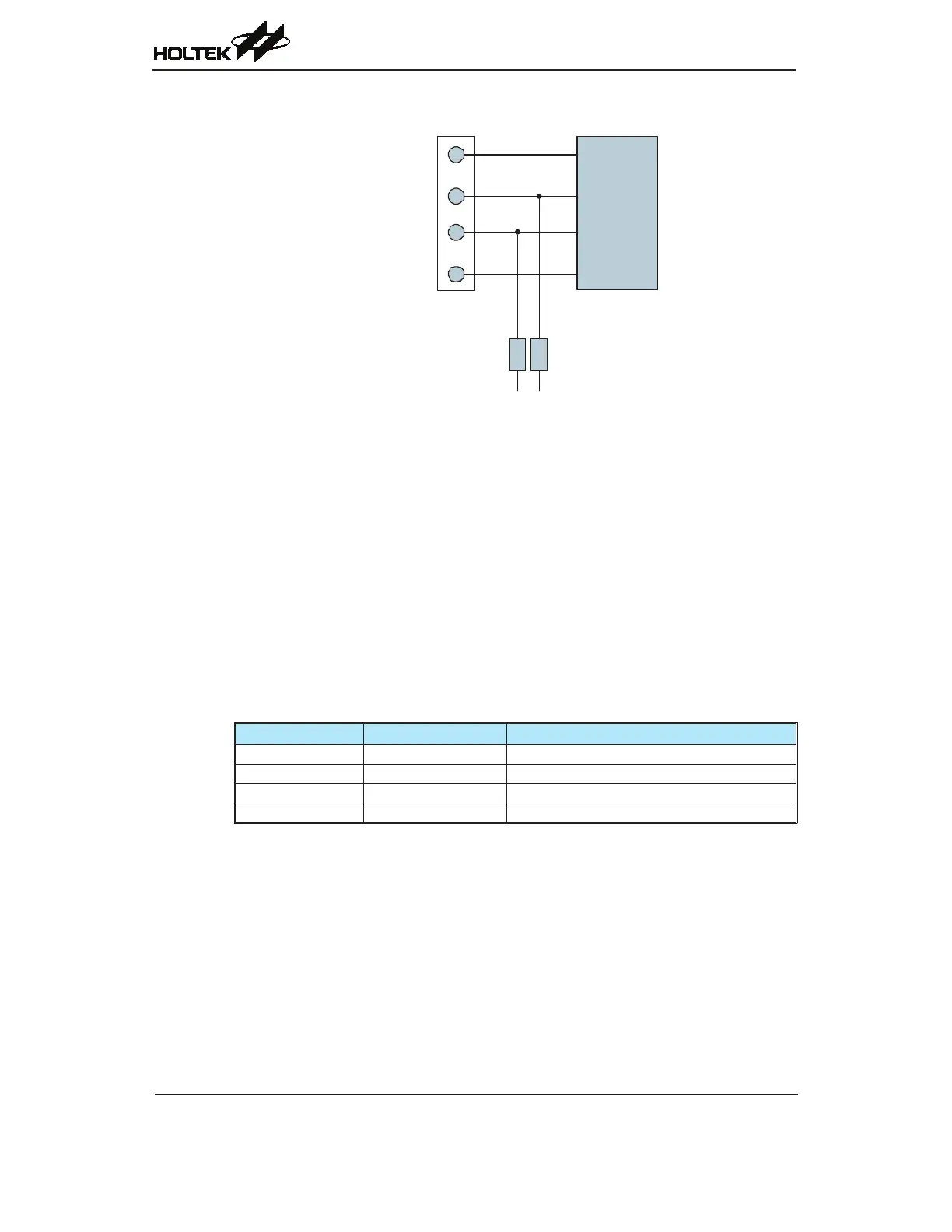
Writer_V DD
IC PDA
IC PCK
Writer_ VSS
PA2
VSS
VDD
Signals
Pins
PA0
Note:*mayberesistororcapacitor.Theresistanceof*mustbegreaterthan1kΩorthecapacitance
of*mustbelessthan1nF.
On-Chip Debug Support – OCDS
ThereisanEVchipnamedHT66V01x5whichisusedtoemulatetherealMCUdevicenamed
HT66F01x5.TheEVchipdevicealsoprovidesthe“On-ChipDebug”functiontodebugthereal
MCUdeviceduringdevelopmentprocess.TheEVchipandrealMCUdevices,HT66V01x5and
HT66F01x5,arealmostfunctionalcompatibleexceptthe“On-ChipDebug”function.Userscan
usetheEVchipdevicetoemulatetherealMCUdevicebehaviorsbyconnectingtheOCDSDA
andOCDSCKpinstotheHoltekHT-IDEdevelopmenttools.TheOCDSDApinistheOCDS
Data/Addressinput/outputpinwhiletheOCDSCKpinistheOCDSclockinputpin.Whenusers
usetheEVchipdevicefordebugging,thecorrespondingpinfunctionssharedwiththeOCDSDA
andOCDSCKpinsintherealMCUdevicewillhavenoeffectintheEVchip.However,thetwo
OCDSpinswhicharepin-sharedwiththeICPprogrammingpinsarestillusedastheFlashMemory
programmingpinsforICP.FormoredetailedOCDSinformation,refertothecorresponding
documentnamed“Holteke-Linkfor8-bitMCUOCDSUser’sGuide”.
Holtek e-Link Pins EV Chip OCDS Pins Pin Description
OCDSDA OCDSDA On-Chip Debug Support Data/Address input/output
OCDSCK OCDSCK On-Chip Debug Support Clock input
VDD VDD Power Supply
VSS VSS Ground