Rev. 1.50 148 August 28, 2017 Rev. 1.50 149 August 28, 2017
HT66F0175/HT66F0185
A/D Flash MCU with EEPROM
HT66F0175/HT66F0185
A/D Flash MCU with EEPROM
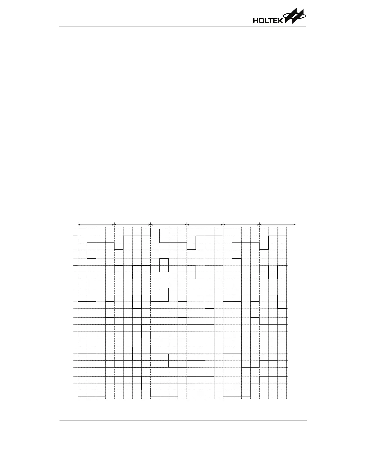
LCD Frames
AcyclicLCDwaveformincludestwoframesknownasFrame0andFrame1forwhichthe
followingoffersafunctionalexplanation.
• Frame 0
ToselectFrame0,cleartheFRAMEbitintheSLCDC0registerto0.
Inframe0,theCOMsignaloutputcanhaveavalueofV
DD
oraV
BIAS
valueof(1/3)×V
DD
.TheSEG
signaloutputcanhaveavalueofV
SS
oraV
BIAS
valueof(2/3)×V
DD
.
• Frame 1
ToselectFrame1,settheFRAMEbitintheSLCDC0registerto1.
Inframe1,theCOMsignaloutputcanhaveavalueofV
SS
oraV
BIAS
valueof(2/3)×V
DD
.TheSEG
signaloutputcanhaveavalueofV
DD
oraV
BIAS
valueof(1/3)×V
DD
.
TheCOMnwaveformiscontrolledbytheapplicationprogramusingtheFRAMEbitinthe
SLCDC0registerandthecorrespondingpin-sharedI/OdatabitfortherespectiveCOMpinto
determinewhethertheCOMnoutputhasavalueofV
DD
,V
SS
orV
BIAS
.TheSEGmwaveformis
controlledinasimilarwayusingtheFRAMEbitandthecorrespondingpin-sharedI/Odatabitfor
therespectiveSEGpintodeterminewhethertheSEGmoutputhasavalueofV
DD
,V
SS
orV
BIAS
.
Theaccompanyingwaveformdiagramshowsatypical1/3biasLCDwaveformgeneratedusingthe
applicationprogramtogetherwiththeLCDvoltageselectcircuit.Notethatthedepictionofa“1”
inthediagramillustratesanilluminatedLCDpixel.TheCOMsignalpolaritygeneratedonpins
SCOM0~SCOM5,whether“0”or“1”,aregeneratedusingthecorrespondingpin-sharedI/Odata
registerbit.
COM0
V
DD
(2/3) V
DD
(1/3) V
DD
V
SS
V
DD
(2/3) V
DD
(1/3) V
DD
V
SS
COM1
COM2
V
DD
(2/3) V
DD
(1/3) V
DD
V
SS
V
DD
(2/3) V
DD
(1/3) V
DD
V
SS
COM3
V
DD
(2/3) V
DD
(1/3) V
DD
V
SS
SEG0
V
DD
(2/3) V
DD
(1/3) V
DD
V
SS
SEG1
Frame 0 Frame 1 Frame 0 Frame 1 Frame 0 Frame 0
1
0
0 0
1
0 0 0
1
0 0 0
1
0 0 0
1
0 0 0
1
0 0
0
1
0 0
0
0 0
1
0
1
0 0
0
0 0
1
0
1
0 0
0 0
1
0 0
1
0
0 0 0
1
0 0
1
0
0 0 0
1
0 0
1
0
0 0
1
0 0 0
1
0
0 0
1
0 0 0
1
0 0 0
1
0 0 0
1
0 0 0
0 0
1 1
0
0
1 1
0 0
1 1
0 0
1 1
0 0
1 1
0 0
1
1 1 1
0
1
1 1
0
1 1 1
0
1 1 1
0
1 1 1
0
1 1 1
Note:Thelogicalvaluesshownintheabovediagramarethecorrespondingpin-sharedI/Odatabitvalue.
1/3 Bias LCD Waveform – 4-COM & 2-SEG application