HP
83522A 83522-90003
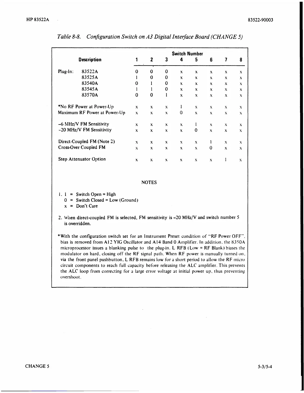
Table
8-8.
Configuration Switch on
A3
Digital Interface Board
(CHANGE
5)
Switch
Number
Description
1
23456
7
8
Plug-In:
83522A 0 0 0
x
x
x
x x
83525A
1
0 0
x x
x x
x
83540A
0
1
0
x
x
x
x
x
83545A
1
1
0
x
x
x
x
x
83570A 0 0
1
x
x x x
s
*No
RF
Power at Power-Up
x x
x
1
x
x
s
.Y
Maximum
RF
Power at Power-Up
x
x
x
0
x
x
s
s
-6
MHz/V FM
Sensitivity
x
x
x
x
1
x
s
s
-20
MHz/V
FM
Sensitivity
x
x
x x
0
x
x s
Direct-Coupled
FM
(Note
2)
x
x
x
x
x
1
x x
Cross-Over Coupled
FM
x
x
x
x
s
0
x
x
Step Attenuator Option
x
x
N
x
s
s
1
s
NOTES
1.
1
=
Switch Open
=
High
0
=
Switch Closed
=
Low (Ground)
x
=
Don't Care
2.
When direct-coupled
FM
is selected,
FM
sensitivity is
-20
MHz/V
and switch number
5
is overridden.
*With the
configuration switch set for an Instrument Preset conditior~ of "RF Power
OFF".
bias is removed from A13 YIG Oscillator and A14 Band
0
Atnplifier. In addition, the
8350A
microprocessor issues a blanking pulse to the plug-in.
L
RFB (Low
=
RF Blank) biases the
niodu!ator on hard, closing off the RF signal path. When RF power is nlanually turned
011.
via the front panel pushbutton,
L
RFB remains low for a short period to allow
the
RF ~llicro
circuit components to reach full capacity before releasing the ALC amplifier. This prevents
the
ALC
loop from correcting for a large error voltage at initial power up.
thus
preventing
overshoot.
A
CHANGE 5