A4 ALC TROUBLESHOOTING (CHANGE
8)
(Cont'd)
4.
To check U2D, monitor U2D pin 10 and TP8 while adjusting the EXT/MTR
ALC CAL
screw between the extremes of its range. Both U2D pin
10
and TP8 should vary between
approximately
+
0.5 and
-
0.5 Vdc.
5.
Verify
U9
by adjusting the CAL screw as described above and monitoring TP5. Since
U9
is an integrator, TP5 should saturate and clamp (due to VR2 and VR3) at
-
7 Vdc
and
+
5 Vdc, respectively.
6.
Remove jumper from A4TPll.
Further troubleshooting of the Modulator Leg can be continued by following the Open Loop
procedure outlined in Figure 8-33 and checking for the waveforms provided in Figure
8-34.
MODULATOR DRIVER
0
The voltage-to-current conversion and current gain needed to drive the modulator is provided
by
42 and Q1 on the output of the Main ALC Amplifier. As the voltage increases at TP5 so does
the current to the modulators, shunting more RF energy to ground and allowing less to pass
through. Since the modulator is essentially current-controlled, the voltages measured at TP6
and
P1-44 do not vary much over a wide range of modulator attenuations.
42 is an emitter-follower followed by a common-base stage (Ql), with two diodes in between.
Check the biases and
baseemitter voltages to see if the transistors are damaged.
To establish a bias level for the Mod Driver state, TP5 can be forced high
(
+
5
Vdc). Jumper
A4TP1 to ground. Press Model
8350A/B
[CW]
and select any
CW
frequency. Select
[EXT]
ALC, and enter an RF power level of
-
2
dBm via front panel controls. Rotate the
EXT/
MTR ALC CAL screw fully counterclockwise. Verify a signal level of approximately
+
5
Vdc at TP5. Remove the jumper from
TP11.
MODULATOR
/
MIXER A17
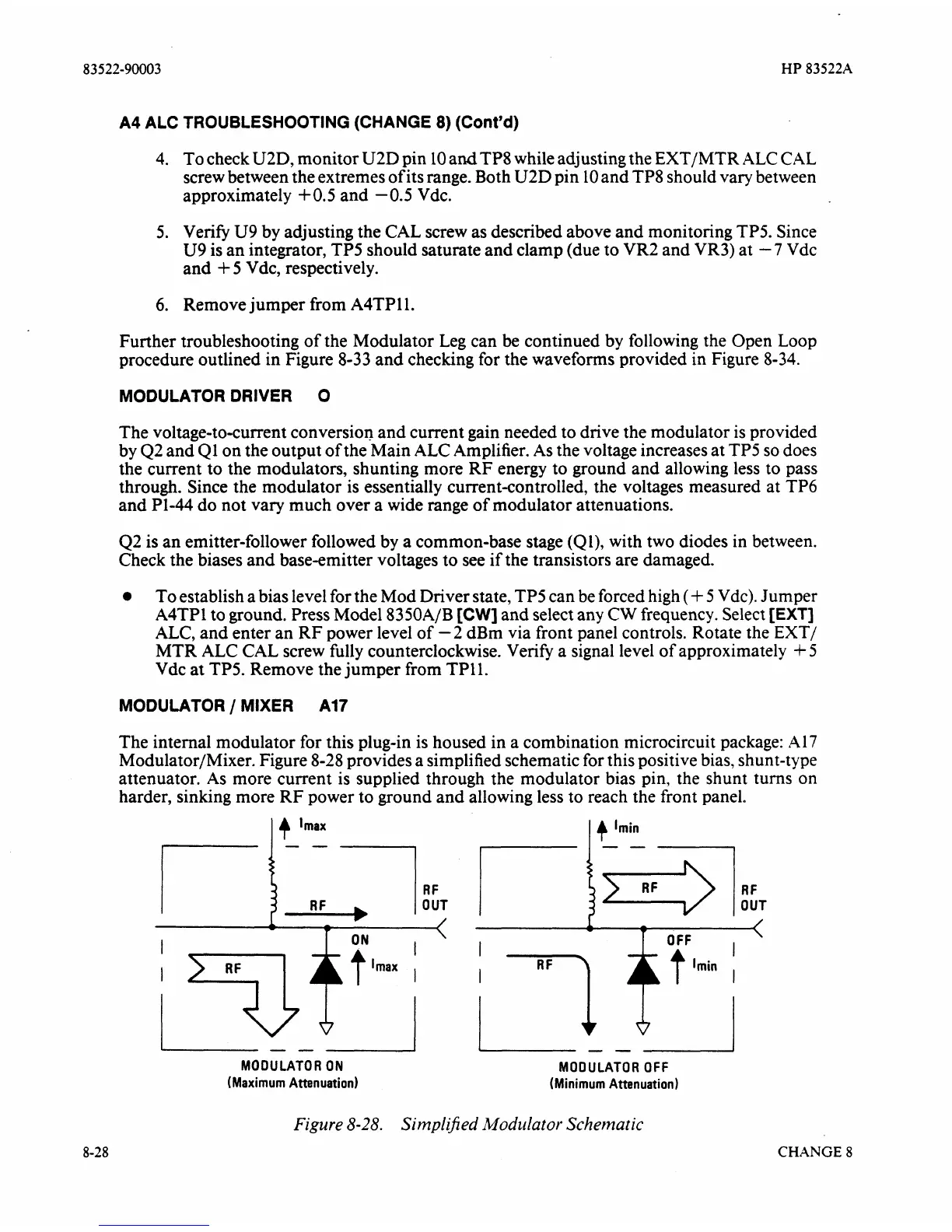
The internal modulator for this plug-in is housed in a combination microcircuit package:
A17
Modulator/Mixer. Figure 8-28 provides a simplified schematic for this positive bias, shunt-type
attenuator. As more current is supplied through the modulator bias pin, the shunt turns
on
harder, sinking more RF power to ground and allowing less to reach the front panel.
-
I
T
OFF
,
\
I
-
-
1
MODULATOR
ON
(Maximum Attenuation)
LI
MODULATOR OFF
(Minimum Attenuation)
Figure
8-28.
Simplified
Modulator
Schematic
CHANGE
8