Model
83522A
Service
-
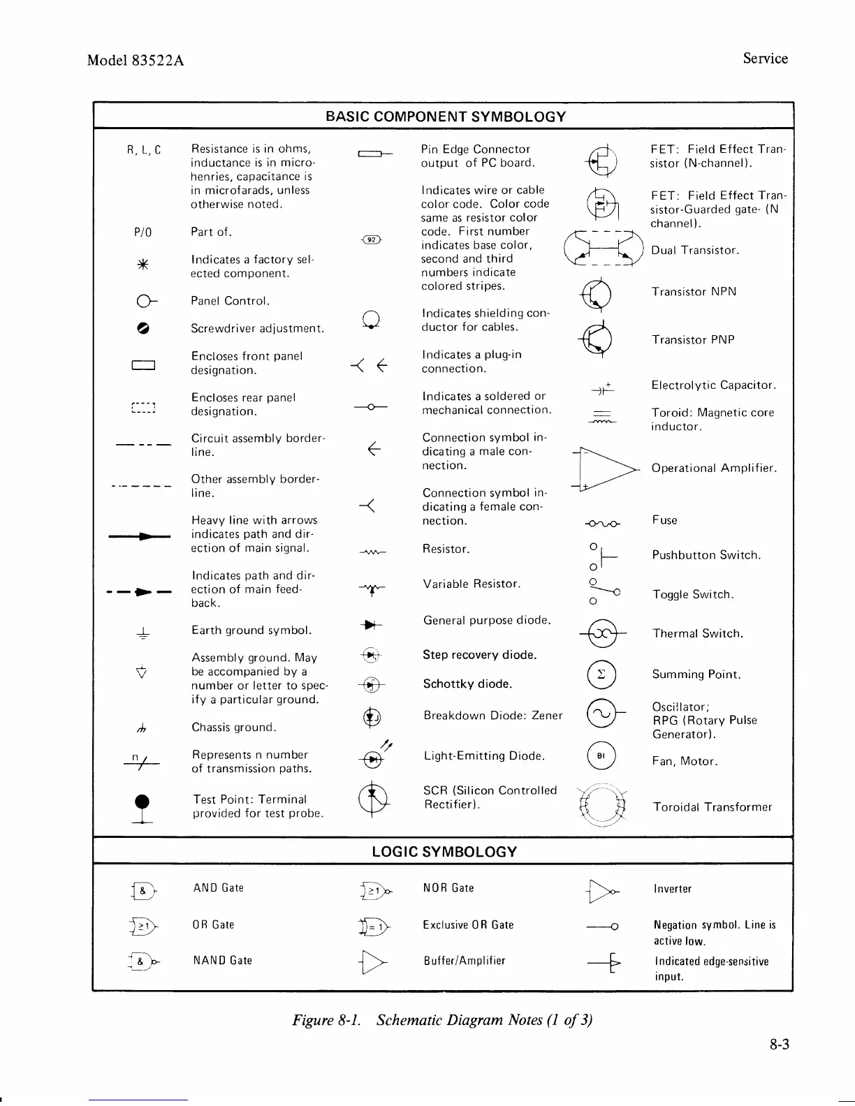
BASIC COMPONENT SYMBOLOGY
R,
L,
C
Resistance is in ohms,
-
Pin Edge Connector FET: Field Effect Tran-
inductance is in micro- output of PC board. sistor (N-channel).
henries, capacitance is
in microfarads, unless Indicates wire or cable
Bl
FET: Field Effect Tran-
otherwise noted. color code. Color code sistor-Guarded gate-
(N
same as resistor color
channel).
PI0 Part of. code. First number
indicates base color,
*
Indicates
a
factory sel-
second and third
o!KQ
Dual Transistor.
ected component. numbers indicate
colored stripes.
Q
Transistor NPN
Panel Control.
lndicates shielding con-
0
Screwdriver adjustment. ductor for cables.
-@
Transistor PNP
Encloses front panel
Indicates a plug-in
designation.
<
connection.
ii
Electrolytic Capacitor.
.----,
Encloses rear panel
lndicates a soldered or
0
&---A
designation.
u
mechanical connection.
- -
Toroid: Magnetic core
-
inductor.
-
--
-
Circuit assembly border-
t
Connection symbol in-
line. dicating
a
male con-
nection.
D
Operational Amplifier.
-.-----
Other assembly border-
line. Connection symbol in-
<
dicating a female con-
Heavy line with arrows nection.
-
Fuse
indicates path and dir-
ection of main signal.
--.A&-
Resistor.
O
Pushbutton Switch.
0
lndicates path and dir-
7-
Variable Resistor.
0
-
-
-
ection of main feed-
back.
Toggle Switch.
0
*
General purpose diode.
&
Earth ground symbol.
@
Thermal Switch.
Assembly ground. May
@
Step recovery diode.
.+
be accompanied by
a
0
Summing Point.
number or letter to spec-
Schottky diode.
ify a particular ground.
@
Breakdown Diode: Zener
/h
Chassis ground.
@
K$!'~~faryPulse Generator).
Represents n number
Light-Emitting Diode.
of transmission paths.
@
Fan, Motor.
@
SCR (Silicon Controlled
Y
Test Point: Terminal Rectifier).
provided for test probe.
r~
Toroidal Transformer
'6
1
LOGIC SYMBOLOGY
AND
Gate
D,
NORGate Inverter
rn
OR
Gate
Exclusive 0
R
Gate
-4
Negation symbol. Line is
active low.
NAND
Gate BufferIArnplifier
-+
l ndicated edge-sensitive
input.
Figure
8-1.
Schematic Diagram Notes
(1
of
3)