Service
Model
83522A
.'
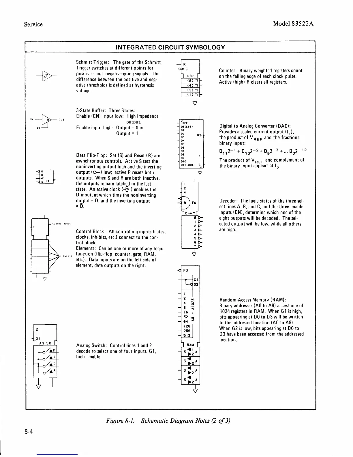
INTEGRATED CIRCUIT SYMBOLOGY
Schmitt Trigger: The gate of the Schmitt
Trigger switches at different points for
+el
Counter: Binary-weighted registers count
positive
-
and negative-going signals. The
on the falling edge of each clock pulse.
difference between the positive and
neg-
Active (high) R clears all registers.
ative thresholds is defined as hysteresis
0)
7
voltage.
(2)
1
3-State Buffer: Three States:
lN
-@-OUT
Enable (EN) Input low: High impedence
output.
Enable input high: Output
=
0 or
DO(LSB)
Fl
Digital to Analog Converter (DAC):
Output
=
1
Provides a scaled current output (I
,),
the product of
V,,,
and the fractional
binary input:
DT
D8
0,,2-'
+
D,,z-2+ 0,~-3
+
...
o0z-l2
Data Flip-Flop: Set (S) and Reset (R) are
D9
asynchronous controls. Active S sets the
DIO
The product of
VREF
and complement of
noninverting output high and the inverting
DII(YSB)
I~
the binary input appears at
I,.
output
(0--1
low; active R resets both
outputs. When S and
R are both inactive,
the outputs remain latched in the last
state. An active clock
(d
enables the
D input, at which time the noninverting
ou_tput
=
D,
and the inverting output
Decoder: The logic states of the three
sel-
=
D.
ect lines A, B, and C, and the three enable
inputs
(EN),
determine which one of the
eight outputs will be decoded. The sel-
ected output will be low, while all others
Control Block: All controlling inputs (gates,
are high.
clocks, inhibits,
etc.) connect to the con-
trol block.
Elements: Can be one or more of any logic
I(tM
function (flip-flop, counter, gate, RAM,
etc.). Data inputs are on the left side of
Figure
8-1.
Schematic Diagram Notes
(2
of
3)
I
Random-Access Memory (RAM):
Binary addresses
(A0 to A91 access one of
1024 registers in RAM. When
GI
is high,
bits appearing at DO to
03 will be written
to the addressed location
(A0 to AS).
When G2 is low, bits appearing at DO to
03 have been accessed from the addressed
location.
element, data outputs on the right.
I,
0
F3
-
I
i
-2
n
-4
nr
-8
:
16
1
32
6,
2
128
266
512
-
I
-
-
2
-
I
-
GI
1
AN-SW
Analog Switch: Control lines
1
and
2
1
RAM
r
J&-
decode to select one of four inputs.
G
1,
high=enable.
-
-
-*3::~
3:;*'
.:;A