Model
83522A
Service
FUNCTION LABEL ABBREVIATIONS
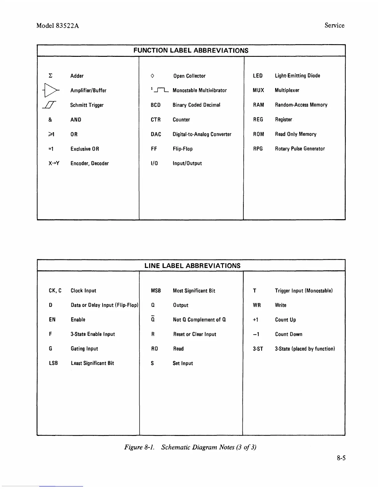
Figure
8-1.
Schematic Diagram Notes
(3
of
3)
8-5
Z1
Adder
u
AmplifierIBuffer
Schmitt Trigger
&
AND
>1
OR
=1
Exclusive
0
R
X-tY Encoder, Decoder
LINE LABEL ABBREVIATIONS
0
Open Collector
'
n
Monostable Multivibrator
BCD Binary Coded Decimal
CTR Counter
DAC Digital-to-Analog Converter
FF Flip-Flop
110 InputIOutput
T Trigger Input (Monostable)
W R Write
+
1
Count Up
-1
Count Down
3-ST 3-State (placed by function)
CK, C Clock Input
D
Data or Delay Input (Flip-Flop)
EN Enable
F 3-State Enable Input
G Gating Input
LSB Least Significant Bit
A
LED Light-Emitting Diode
MUX Multiplexer
RAM Random-Access Memory
REG Register
ROM Read Only Memory
RPG Rotary Pulse Generator
MSB Most Significant Bit
Q
Output
-
Q
Not
Q
Complement of
Q
R Reset or Clear Input
RD Read
S Set Input