Model
83522A
Service
Further troubleshooting of the Modulator Leg can be continued by following
the Open Loop procedure outlined in Figure 8-33 and checking for the
waveforms provided in Figure 8-34.
Modulator Driver
@
The PIN Mod 0 Driver provides the voltage-to-current conversion and current
gain needed to drive the modulator. As the voltage increases at TP6 so does the
current to the Modulator, shunting more RF energy to ground and allowing less
to pass through. Since the modulator is essentially current-controlled, the
voltages measured at
TP8 and P1-44 do not vary much over a wide range of
modulator attenuations.
The PIN Mod
0 Driver is an emitter-follower followed by a common-base stage,
with two diodes in between. Check the biases and base-emitter voltages to check
for damaged transistors.
To establish a bias level for the PIN Mod 0 Driver, TP6 can be forced high
(4-7.5
Vdc) by pressing 8350A
CW
and selecting any CW frequency.
Select
EXT
ALC, and enter an RF power level of
-2
dBm via front panel
controls. Ground
A4TPll. Rotate the EXTIMTR ALC
CAL
knob fully
counter-clockwise to set a signal level of approximately
+7.5
Vdc at TP6.
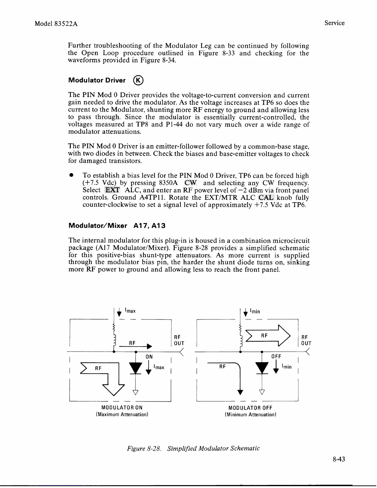
The internal modulator for this plug-in is housed in a combination microcircuit
package (A17
ModulatorIMixer). Figure 8-28 provides a simplified schematic
for this positive-bias shunt-type attenuators. As more current is supplied
through the modulator bias pin, the harder the shunt diode turns on, sinking
more RF power to ground and allowing less to reach the front panel.
MODULATOR
ON
(Maximum Attenuation)
1
I
T
OFF
I
MODULATOR OFF
(Minimum Attenuation)
Figure
8-28.
Simplified Modulator Schematic
 Loading...


