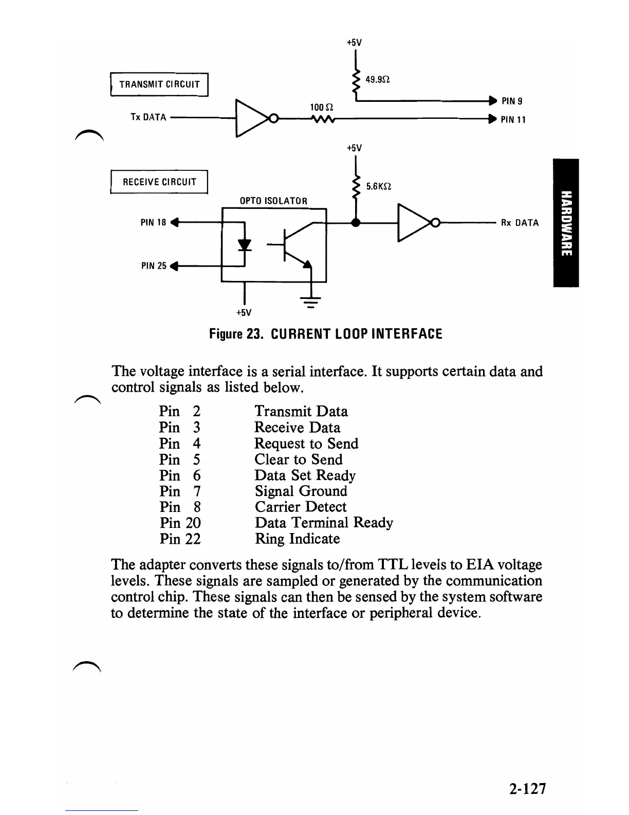
+5V
I
TRANSMIT
'IACUIT
I
~
4S-"l
Tx
DATA
----I~.,..-----------.,:~
:11::
1
+5V
RECEIVE
CIRCUIT
5.SK.I1
OPTO
ISOLATOR
PIN
18
4---t-.,
:>0---
Rx
DATA
PIN
25
"'
__
+--J
+5V
Figure
23.
CURRENT
LOOP
INTERFACE
The voltage interface
is
a serial interface.
It
supports certain data and
control signals
as
listed below.
~
Pin 2 Transmit
Data
Pin 3 Receive Data
Pin 4 Request to Send
Pin 5 Clear to Send
Pin 6 Data Set Ready
Pin 7 Signal Ground
Pin 8 Carrier Detect
Pin 20 Data Terminal Ready
Pin 22 Ring Indicate
The adapter converts these signals to/from
TTL
levels to
EIA
voltage
levels. These signals are sampled or generated by the communication
control chip. These signals can then
be
sensed by the system software
to determine the state
of
the interface or peripheral device.
2-127
 Loading...