Bit 0: This bit
is
the Delta Clear to Send (DCTS) indicator. Bit 0
indicates that the CTS input to the chip has changed state since the last
time it was read by the CPU.
Bit
1:
This bit
is
the Delta
Data
Set Ready (DDSR) indicator. Bit 1
indicates that the
DSR
input to the chip has changed state since the last
~~~re~~~~ll
~
Bit
2:
This bit
is
the Trailing Edge
of
Ring Indicator (TERI) detector.
Bit 2 indicates that the RI input to the chip has changed from an On
(logic
1)
to an Off (logic 0) condition.
Bit
3:
This bit
is
the Delta Received Line Signal Detector (DRLSD)
indicator. Bit 3 indicates that the RLSD input to the chip has changed
state.
Note: Whenever bit 0,
1,
2,
or
3
is
set to a logic
1,
a
MODEM
Status
interrupt
is
generated.
Bit4: This bit
is
the complement
of
the Clear to Send (CTS) input. Ifbit
4 (loop) of the
MCR
is set to a
1,
this bit
is
equivalent to RTS in the
MCR
Bit
5:
This bit
is
the complement ofthe
Data
Set Ready (DSR) input.
If
bit 4
of
the
MCR
is
set to
ai,
this bit is equivalent to
DTR
in the
MCR
Bit
6:
This bit
is
the complement ofthe Ring Indicator (RI) input. Ifbit 4
r-...
of the M
CR
is set to
aI,
this bit is equivalent to
OUT
1 in the M
CR
Bit 7: This bit
is
the complement
of
the Received Line Signal Detect
(RLSD) input.
If
bit 4
of
the
MCR
is
set to
ai,
this bit
is
equivalent to
OUT
2
of
the
MCR
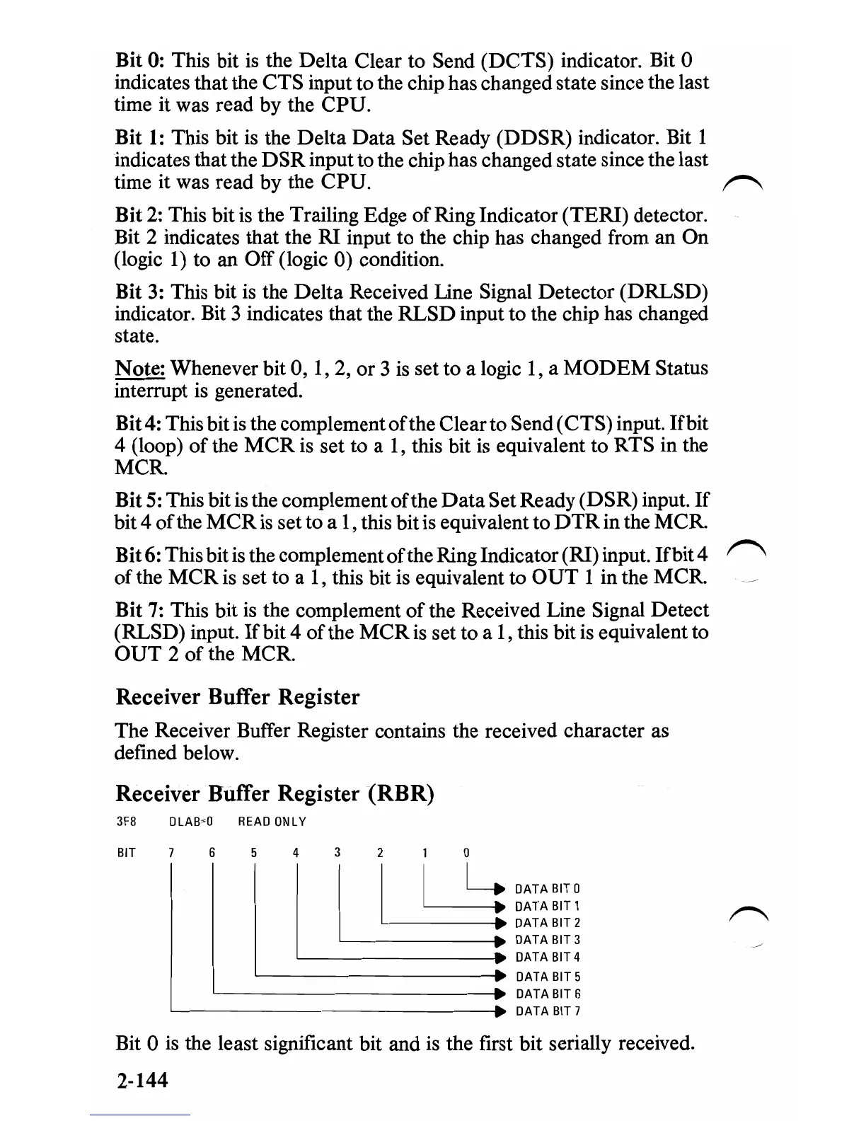
Receiver Buffer Register
The Receiver Buffer Register contains the received character as
defined below.
Receiver Buffer Register
(RBR)
3F8
DLAB;O
READ
ONLY
BIT
4 3 2 1 0
I
1,----1
________
m~ml
~~
'---.
--------:.
DATABIT4
'-----------.
DATABIT5
'-----------------.
DATA
BIT
6
'-----------------..
DATA
BIT
7
Bit 0
is
the least significant bit and
is
the first bit serially received.
2-144

 Loading...