INS8250 Accessible Registers
The system programmer may access
or
control any
of
the INS8250
registers via the
CPU.
These registers are used to control INS8250
operations and to transmit and receive data.
INS8250 Line Control Register
The system programmer specifies the format
of
the asynchronous data
communications exchange via the Line Control Register. In addition to
controlling the format, the programmer may retrieve the contents
of
the
Line Control Register for inspection. This feature simplifies system
programming and eliminates the need for separate storage in system
memory
of
the line characteristics.
The
contents
of
the Line Control
Register are indicated and described below.
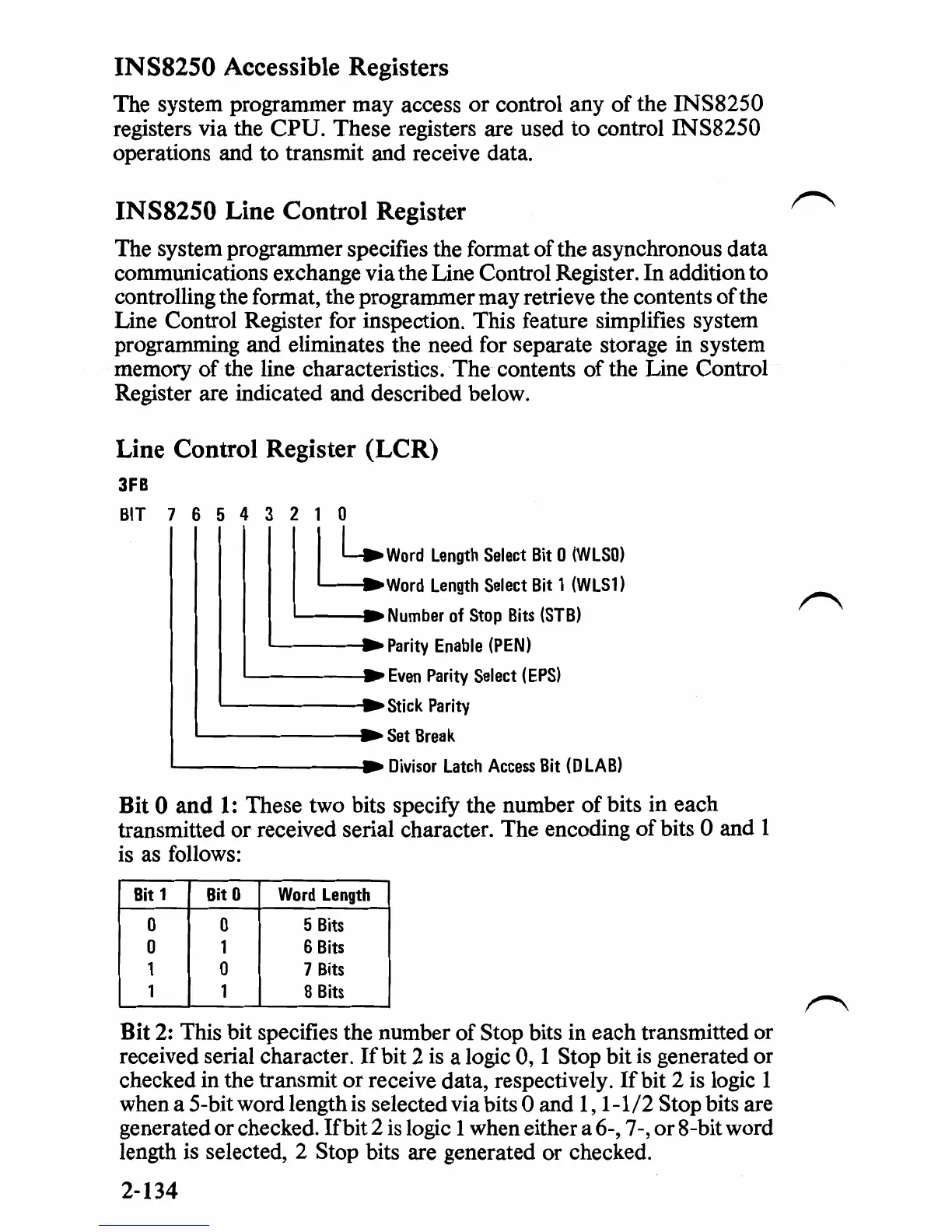
Line Control Register (LCR)
3FB
BIT
7 6 5 4 3 2 1 0
I' I :
Word
L,"gth
SoI,01
Bit
D
IW
LSD)
Word
Length
Select
Bit
1
(WLS1)
Number
of
Stop
Bits
(STB)
~--~Parity
Enable
(PEN)
'------~Even
Parity
Select
(EPS)
'-------~Stick
Parity
L--
_____
~
Set
Break
L--
______
....
Divisor
Latch
Access
Bit
(DLAB)
Bit 0
and
1:
These two bits specify the number
of
bits in each
transmitted or received serial character. The encoding
of
bits 0 and 1
is as follows:
Bit
1
Bit
0
Word
Length
0
0 5
Bits
0 1 6
Bits
1
0 7
Bits
1 1
8
Bits
Bit 2: This bit specifies the number
of
Stop bits in each transmitted or
received serial character.
If
bit 2
is
a logic 0, 1 Stop bit is generated or
checked in the transmit
or
receive data, respectively.
Ifbit
2 is logic 1
when a 5-bit word length is selected via bits 0 and 1, 1-1/2 Stop bits are
generated
or
checked. Ifbit 2
is
logic 1 when either a 6-, 7-,
or
8-bit word
length
is
selected, 2 Stop bits are generated or checked.
2-134
 Loading...