4-7
4-3
FREQUENCY SYNTHESIZER CIRCUITS
(MAIN UNIT)
VCOs
The IC-2730A/E has total of four VCOs: two VCOs for the left
band and another two for the right band.
• Left band
VHF VCO
The VHF VCO (Q211, D203, D204, D206, D228 and D342)
generates the VHF TX signal. The output of buffer (Q215) is
amplifi ed by the LO AMP (Q240), and then applied to the
VHF TX AMP circuit, through the LO SW (D50).
UHF VCO
The UHF VCO (Q210, D201, D202 and D205) generates the
1st LO signal (for receiving a UHF signal on the left band).
The output of buffer (Q214) is amplifi ed by the LO AMP
(Q240), and then applied to the 1st IF mixer (Q146), through
the LO SW (D213) and LPF (L315, C988 and C995).
• Right band
VHF VCO
The VHF VCO (Q233, D225, D226 and D230) generates the
1st LO signal (for receiving a VHF signal on the right band).
The output of buffer (Q236) is amplifi ed by the LO AMP
(Q238), and then applied to the 1st IF mixer (Q143), through
the LO SW (D235) and LPF (L338, L339, C1105 and
C1106).
UHF VCO
The UHF VCO (Q232, D223, D224, D227, D229 and D236)
generates the UHF TX signal. The output of buffer (Q235) is
applied to the UHF TX AMP circuit.
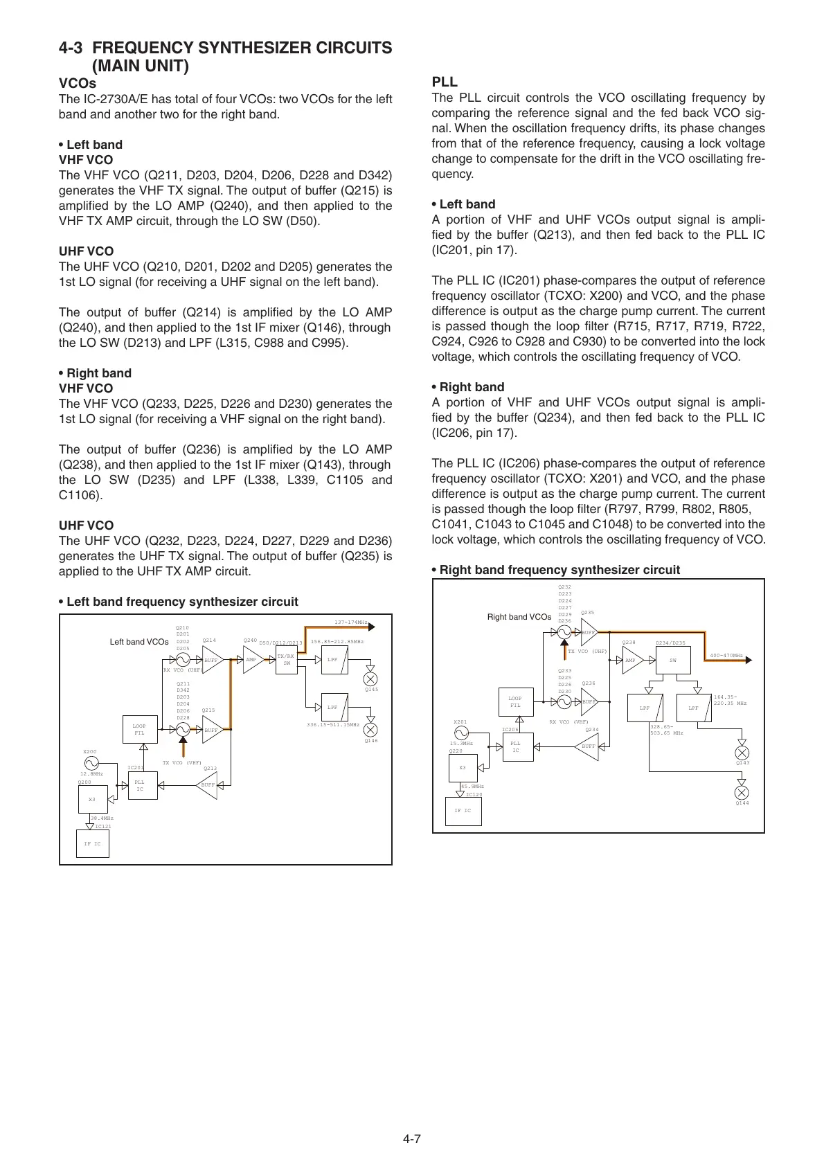
• Left band frequency synthesizer circuit
AMP
BUFF
BUFF
BUFF
LPF
LPF
TX/RX
SW
X3
FIL
LOOP
PLL
IC
IF IC
Left band VCOs
38.4MHz
12.8MHz
X200
IC201
Q200
Q213
Q215
Q211
Q210
Q214
Q240
TX VCO (VHF)
RX VCO (UHF)
D50/D212/D213
IC121
Q146
Q145
D201
D202
D203
D204
D206
D342
D228
D205
137-174MHz
156.85-212.85MHz
336.15-511.15MHz
PLL
The PLL circuit controls the VCO oscillating frequency by
comparing the reference signal and the fed back VCO sig-
nal. When the oscillation frequency drifts, its phase changes
from that of the reference frequency, causing a lock voltage
change to compensate for the drift in the VCO oscillating fre-
quency.
• Left band
A portion of VHF and UHF VCOs output signal is ampli-
fi ed by the buffer (Q213), and then fed back to the PLL IC
(IC201, pin 17).
The PLL IC (IC201) phase-compares the output of reference
frequency oscillator (TCXO: X200) and VCO, and the phase
difference is output as the charge pump current. The current
is passed though the loop fi lter (R715, R717, R719, R722,
C924, C926 to C928 and C930) to be converted into the lock
voltage, which controls the oscillating frequency of VCO.
• Right band
A portion of VHF and UHF VCOs output signal is ampli-
fi ed by the buffer (Q234), and then fed back to the PLL IC
(IC206, pin 17).
The PLL IC (IC206) phase-compares the output of reference
frequency oscillator (TCXO: X201) and VCO, and the phase
difference is output as the charge pump current. The current
is passed though the loop fi lter (R797, R799, R802, R805,
C1041, C1043 to C1045 and C1048) to be converted into the
lock voltage, which controls the oscillating frequency of VCO.
• Right band frequency synthesizer circuit
AMP
FIL
LOOP
BUFF
BUFF
BUFF
PLL
IC
LPFLPF
X3
IF IC
15.3MHz
Right band VCOs
45.9MHz
X201
IC206
Q220
Q234
Q236
Q233
TX VCO (UHF)
RX VCO (VHF)
Q232
Q235
Q238
D234/D235
IC120
Q144
Q143
SW
D223
D224
D225
D226
D227
D229
D230
D236
400-470MHz
164.35-
220.35 MHz
328.65-
503.65 MHz