Electrical
613768 41
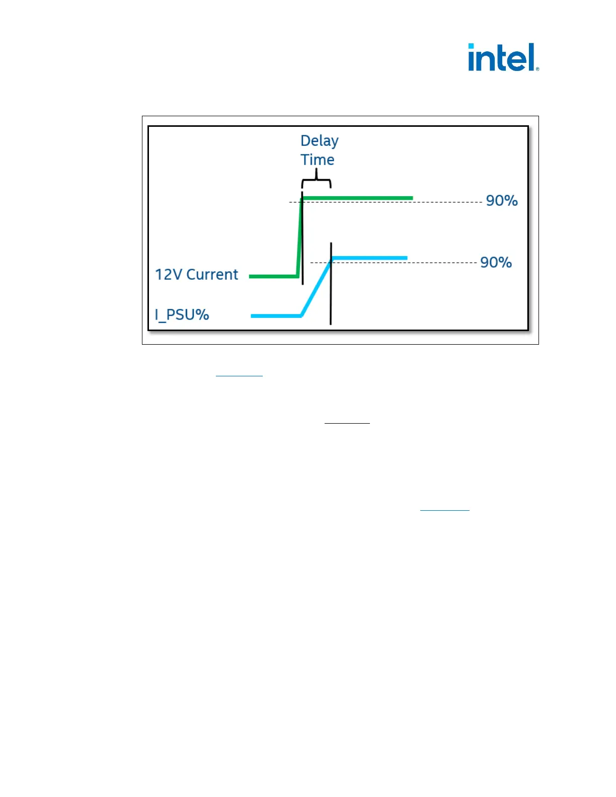
Figure 4-6: I_PSU% Delay Time Diagram
Inside the power supply, a transconductance amplifier needs to be added to report the
I_PSU% signal. Figure 4-7
below is a reference schematic for the circuitry that needs
to be included. The green box represents the power supply. For the transconductance
amplifier the Iout equation of I_PSU% is shown here:
=
∗
The Figure shows the Total 12V Main output that represents all power connectors to
the system. The diagram is simplified to show all load with just I1.
The I_PSU% signal is routed to the Psys pin on the CPU’s IMVP controller on the
motherboard. Also, on the motherboard is RL and CL, which are in parallel with each
other and placed as close to the IMVP controller as possible. Table 4-11
shows the
range of values that RL and CL should be. Capacitor recommendation is C0G (NP0)
type. Resistors are recommended to be 1% type and capacitor are recommended to
be 5% type.
For all Accuracy, Delay Time and Ripple/Noise measurements, testing is to be
completed with both the RL_low + CL_low and RL_high + CL_high combinations.
When calculating the value for C3 the I_PSU% Delay time requirements need to be
considered.