Datasheet 107
Intel
®
Celeron
®
Processor up to 1.10 GHz
NOTES:
1. VCC
1.5
must be supplied by the same voltage
source supplying V
TT on the motherboard.
2. Previously this pin functioned as the EDGCTRL
signal.
3. Previously, PGA370 designs defined this pin as a
GND. For flexible PGA370 designs, it must be left
unconnected (NC).
4. Previously, PGA370 designs defined this pin as a
GND.
5. Celeron processor in the FC-PGA/FC-PGA2
packages does not make use of this pin.
6. This pin is only reset for processors with a CPUID
of 0686h. For previous Celeron processors prior
to 0686h (not including 0686h) this pin is
reserved.
7. This pin is reserved for Celeron processors with a
CPUID of 0686h.
8. For CPUID of 0681h, this is a V
SS. For other
068xh processors, this pin is a No Connect (NC).
Q5 GND Power/Other
Q33 Reserved Reserved for future use
Q35 Reserved Reserved for future use
Q37 Reserved Reserved for future use
R2 Reserved Reserved for future use
R4 D17# AGTL+ I/O
R6 V
REF3 Power/Other
R32 V
CC
CORE
Power/Other
R34 GND Power/Other
R36 V
CC
CORE
Power/Other
S1 D8# AGTL+ I/O
S3 D5# AGTL+ I/O
S5 V
CC
CORE
Power/Other
S33 Reserved Reserved for future use
S35 RTTCTRL Power/Other
S37 Reserved Reserved for future use
T2 V
CC
CORE
Power/Other
T4 D1# AGTL+ I/O
T6 D6# AGTL+ I/O
T32 GND Power/Other
T34 V
CC
CORE
Power/Other
T36 GND Power/Other
U1 D4# AGTL+ I/O
U3 D15# AGTL+ I/O
U5 GND Power/Other
U33 PLL2 Power/Other
U35 Reserved Reserved for future use
U37 Reserved Reserved for future use
V2 GND Power/Other
V4 Reserved Reserved for future use
V6 V
REF4 Power/Other
V32 V
CC
CORE
Power/Other
V34 GND Power/Other
V36 V
CC
CORE
Power/Other
W1 D0# AGTL+ I/O
W3 Reserved Reserved for future use
W5 V
CC
CORE
Power/Other
W33 PLL1 Power/Other
W35 Reserved Reserved for future use
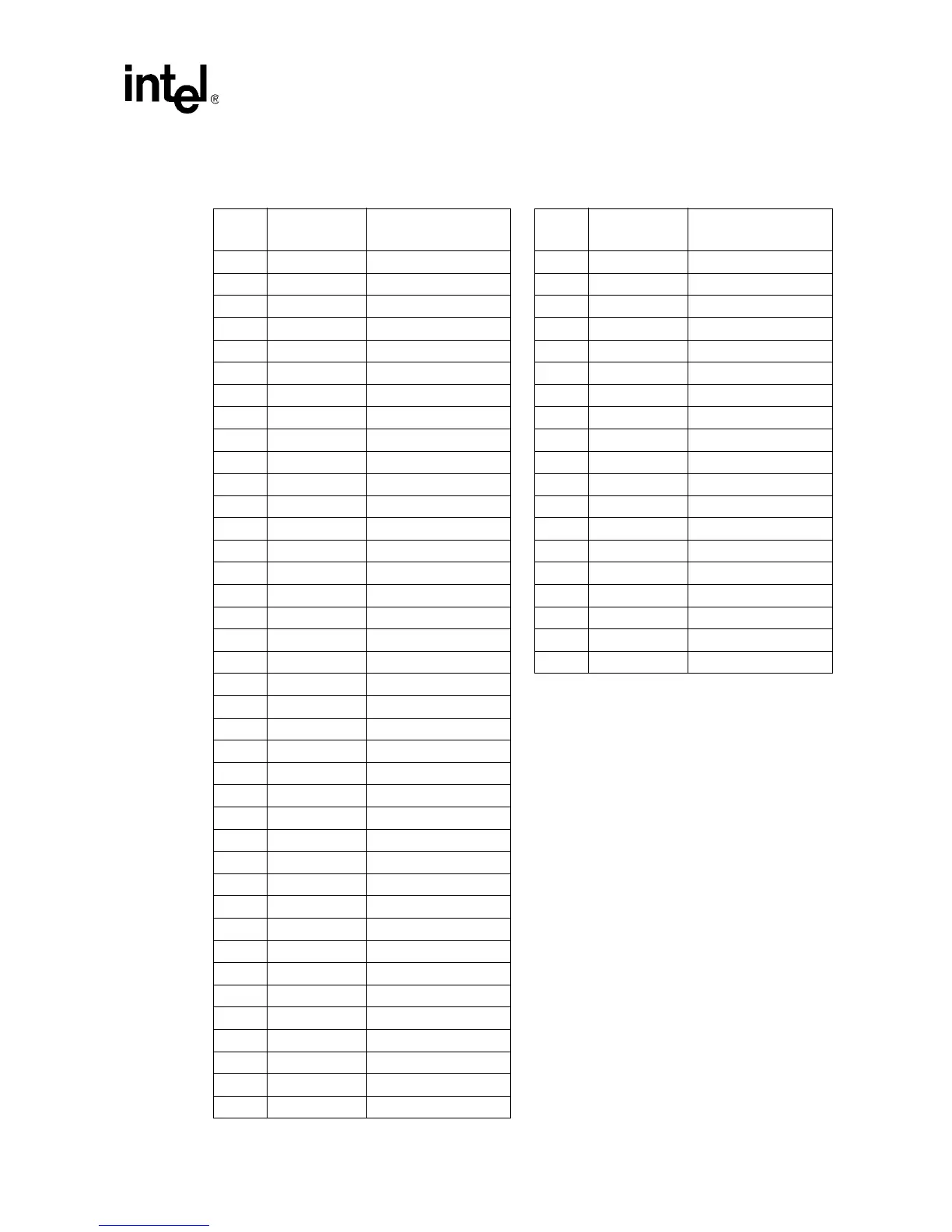
Table 56. FC-PGA/FC-PGA2 Signal
Listing in Order by Pin
Number
Pin
No.
Pin Name Signal Group
W37 BCLK System Bus Clock
X4 RESET#
7
Power/Other
X6 Reserved Reserved for future use
X20 Reserved Reserved for future use
X32 GND Power/Other
X34 Reserved Reserved for future use
X36 GND Power/Other
Y1 Reserved Reserved for future use
Y3 A26# AGTL+ I/O
Y5 GND Power/Other
Y33 Reserved
4
Reserved for future use
Y35 V
CC
CORE
Power/Other
Y37 GND Power/Other
Z2 GND Power/Other
Z4 A29# AGTL+ I/O
Z6 A18# AGTL+ I/O
Z32 V
CC
CORE
Power/Other
Z34 GND Power/Other
Z36 Vcc
2.5
Power/Other
Table 56. FC-PGA/FC-PGA2 Signal
Listing in Order by Pin
Number
Pin
No.
Pin Name Signal Group
 Loading...