EasyManua.ls Logo

Intel CELERON 1.10 GHZ User Manual

Intel CELERON 1.10 GHZ
128 pages
To Next Page IconTo Next Page
Page #1 background imageLoading...
Page #1 background image
Intel
®
Celeron
®
Processor
up to 1.10 GHz
Datasheet
The Intel
®
Celeron
®
processor is designed for uni-processor based Value PC desktops and is
binary compatible with previous generation Intel architecture processors. The Celeron processor
provides good performance for applications running on advanced operating systems such as
Microsoft* Windows*98, Windows NT*, Windows* 2000, Windows XP* and Linux*. This is
achieved by integrating the best attributes of Intel processors—the dynamic execution
performance of the P6 microarchitecture plus the capabilities of MMX™ technology—bringing
a balanced level of performance to the Value PC market segment. The Celeron processor offers
the dependability you would expect from Intel at an exceptional value. Systems based on
Celeron processors also include the latest features to simplify system management and lower the
cost of ownership for small business and home environments.
Available at 1.10 GHz, 1 GHz, 950 MHz,
900 MHz, 850 MHz, 800 MHz, 766 MHz,
733 MHz, 700 MHz, 667 MHz, 633 MHz,
600 MHz, 566 MHz, 533 MHz,
533A MHz, 500 MHz, 466 MHz,
433 MHz, 400 MHz, 366 MHz, 333 MHz,
and 300A MHz core frequencies with
128 KB level-two cache (on die); 300 MHz
and 266 MHz core frequencies without
level-two cache.
Intel’s latest Celeron
®
processors in the
FC-PGA/FC-PGA2 package are
manufactured using the advanced 0.18
micron technology.
Binary compatible with applications
running on previous members of the Intel
microprocessor line.
Dynamic execution microarchitecture.
Operates on a 100/66 MHz, transaction-
oriented system bus.
Specifically designed for uni-processor
based Value PC systems, with the
capabilities of MMX™ technology.
Power Management capabilities.
Optimized for 32-bit applications running
on advanced 32-bit operating systems.
Uses cost-effective packaging technology.
Single Edge Processor (S.E.P.) Package
to maintain compatibility with SC242
(processor core frequencies (MHz):
266, 300, 300A, 333, 366, 400, 433).
Plastic Pin Grid Array (PPGA) Package
(processor core frequencies (MHz):
300A, 333, 366, 400, 433, 466, 500,
533).
Flip-Chip Pin Grid Array (FC-PGA /
FC-PGA2) Package (processor core
frequencies (MHz); 533A, 566, 600,
633, 667, 700, 733, 766, 800, 850, 900,
950); (GHz); 1, 1.10
Integrated high-performance 32 KB
instruction and data, nonblocking, level-
one cache: separate 16 KB instruction and
16 KB data caches.
Integrated thermal diode.
S.E.P. PackageFC-PGA2 Package FC-PGA Package
PPGA Package
Document Number: 243658-020
January 2002

Table of Contents

Question and Answer IconNeed help?

Do you have a question about the Intel CELERON 1.10 GHZ and is the answer not in the manual?

Intel CELERON 1.10 GHZ Specifications

General IconGeneral
ModelIntel Celeron 1.10 GHz
Base Clock Speed1.10 GHz
Cores1
Threads1
Socket TypeSocket 370
Lithography180 nm
Manufacturing Process180 nm

Summary

1.0 Introduction

1.1 Terminology

Defines terms used in the document, including signal naming conventions.

1.1.1 Package Terminology

Explains terminology related to processor packages like S.E.P., PPGA, FC-PGA, and FC-PGA2.

1.1.2 Processor Naming Convention

Details the naming conventions for Intel Celeron processors and their identification.

1.2 References

2.0 Electrical Specifications

2.1 System Bus and VREF

Explains the GTL signaling technology and VREF usage for system bus signals.

2.2 Clock Control and Low Power States

Describes processor power states and clock control mechanisms for power saving.

2.2.1 Normal State—State 1

Describes the standard operating state of the processor.

2.2.2 AutoHALT Power Down State—State 2

Details the AutoHALT power-down state entered via the HALT instruction.

2.2.3 Stop-Grant State—State 3

Explains the Stop-Grant state entered when STPCLK# is asserted.

2.2.4 HALT/Grant Snoop State—State 4

Describes the state entered during snoop transactions while in Stop-Grant or AutoHALT.

2.2.5 Sleep State—State 5

Details the very low power Sleep state that maintains context.

2.2.6 Deep Sleep State—State 6

Describes the lowest power Deep Sleep state entered by stopping BCLK input.

2.2.7 Clock Control

Explains the role of BCLK and PICCLK in processor operation and power states.

2.3 Power and Ground Pins

Details the power and ground pins used for voltage identification and power distribution.

2.3.1 Phase Lock Loop (PLL) Power

Highlights the critical requirement for PLL power delivery with a low pass filter.

2.4 Processor Decoupling

Explains the need for decoupling capacitance to manage current swings.

2.4.1 System Bus AGTL+ Decoupling

Discusses high-frequency decoupling requirements for AGTL+ bus operation.

2.5 Voltage Identification

Describes the VID pins used for automatic VCCCORE voltage selection.

2.6 System Bus Unused Pins

Advises on handling and connecting unused processor pins to avoid malfunctions.

2.7 Processor System Bus Signal Groups

Groups Celeron processor system bus signals by buffer type for discussion.

2.7.1 Asynchronous Vs. Synchronous for System Bus Signals

Differentiates synchronous and asynchronous signal behavior on the system bus.

2.7.2 System Bus Frequency Select Signal (BSEL[1:0])

Explains the function of BSEL pins for selecting system bus frequency.

2.8 Test Access Port (TAP) Connection

Provides recommendations for connecting to the Test Access Port logic.

2.9 Maximum Ratings

Lists the absolute maximum and minimum ratings for the Celeron processor.

2.10 Processor DC Specifications

Details the DC specifications for the Celeron processor, including AGTL+ and CMOS signals.

2.11 AGTL+ System Bus Specifications

Specifies AGTL+ bus routing and termination requirements.

2.12 System Bus AC Specifications

Defines system bus timings at processor edge fingers and core pins.

3.0 System Bus Signal Simulations

3.1 System Bus Clock (BCLK) Signal Quality Specifications and Measurement Guidelines

Provides BCLK signal quality specifications and measurement guidelines.

3.1.1 BCLK Signal Quality Specifications for Simulation at the Processor Core

Lists BCLK signal quality specifications for simulation at the processor core.

3.2 AGTL+ Signal Quality Specifications and Measurement Guidelines

Provides AGTL+ signal quality specifications and measurement guidelines.

3.2.1 AGTL+ Signal Groups Ringback Tolerance Specifications at the Processor Core

Lists AGTL+ signal ringback tolerance specs at the processor core for S.E.P. and PPGA.

3.2.2 AGTL+ Signal Groups Ringback Tolerance Specifications at the Processor Pins

Lists AGTL+ signal ringback tolerance specs at processor pins for FC-PGA/FC-PGA2.

3.3 Non-AGTL+ Signal Quality Specifications and Measurement Guidelines

Details non-AGTL+ signal quality parameters: overshoot, ringback, and settling limit.

3.3.1 Overshoot/Undershoot Guidelines

Explains overshoot/undershoot guidelines and potential damage from violations.

3.3.2 Ringback Specification

Defines ringback as a reflection seen after signal switching and its impact.

3.3.3 Settling Limit Guideline

Defines settling limit as maximum ringing before next transition.

3.4 AGTL+ Signal Quality Specifications and Measurement Guidelines (FC-PGA/FC-PGA2 Packages)

Provides AGTL+ signal quality specs and measurement guidelines for FC-PGA/FC-PGA2.

3.4.1 Overshoot/Undershoot Guidelines (FC-PGA/FC-PGA2 Packages)

Explains overshoot/undershoot guidelines for FC-PGA/FC-PGA2 packages.

3.4.2 Overshoot/Undershoot Magnitude (FC-PGA/FC-PGA2 Packages)

Describes overshoot/undershoot magnitude measurement for FC-PGA/FC-PGA2 packages.

3.4.3 Overshoot/Undershoot Pulse Duration (FC-PGA/FC-PGA2 Packages)

Defines pulse duration for overshoot/undershoot events for FC-PGA/FC-PGA2 packages.

3.4.4 Activity Factor (FC-PGA/FC-PGA2 Packages)

Explains Activity Factor and its relevance to signal quality for FC-PGA/FC-PGA2.

3.4.5 Reading Overshoot/Undershoot Specification Tables (FC-PGA/FC-PGA2 Packages)

Guides on how to read overshoot/undershoot specification tables for FC-PGA/FC-PGA2.

3.4.6 Determining if a System meets the Overshoot/Undershoot Specifications (FC-PGA/FC-PGA2 Packages)

Provides guidelines to determine if a system meets overshoot/undershoot specifications.

3.5 Non-AGTL+ Signal Quality Specifications and Measurement Guidelines

Details non-AGTL+ signal quality parameters: overshoot, ringback, and settling limit.

4.0 Thermal Specifications and Design Considerations

4.1 Thermal Specifications

Details processor power and heatsink design targets and case temperatures.

4.1.1 Thermal Diode

Explains the on-die thermal diode used for monitoring die temperature.

5.0 Mechanical Specifications

5.1 S.E.P. Package

Defines mechanical specifications and signal definitions for the S.E.P. Package.

5.1.1 Materials Information

Describes retention mechanism requirements and substrate dimensions for S.E.P. package.

5.1.2 Signal Listing (S.E.P. Package)

Provides signal definitions and locations for the S.E.P. package edge connector.

5.2 PPGA Package

Defines mechanical specifications and signal definitions for the PPGA package.

5.2.1 PPGA Package Materials Information

Provides information for designing a heatsink and clip for the PPGA package.

5.2.2 PPGA Package Signal Listing

Provides a pin-side view and listing of signals for the PPGA package.

5.3 FC-PGA/FC-PGA2 Packages

Defines mechanical specifications and signal definitions for FC-PGA and FC-PGA2 packages.

5.3.1 FC-PGA Mechanical Specifications

Provides package dimensions and pin-side capacitor locations for the FC-PGA package.

5.3.2 Mechanical Specifications (FC-PGA2 Package)

Provides package dimensions and pin-side capacitor locations for the FC-PGA2 package.

5.3.2.1 Recommended Mechanical Keep-Out Zones (FC-PGA2 Package)

Illustrates volumetric and component keep-out zones for the FC-PGA2 package.

5.3.3 FC-PGA/FC-PGA2 Package Signal List

Provides pin definitions and a pin-side view for FC-PGA/FC-PGA2 packages.

5.4 Processor Markings (PPGA/FC-PGA/FC-PGA2 Packages)

Shows processor top-side markings for identification purposes.

5.5 Heatsink Volumetric Keepout Zone Guidelines

Provides guidelines for ensuring sufficient space for heatsink installation without interference.

6.0 Boxed Processor Specifications

6.1 Mechanical Specifications for the Boxed Intel® Celeron® Processor

Details mechanical specifications for boxed Intel Celeron processors and their heatsinks.

6.1.1 Mechanical Specifications for the S.E.P. Package

Documents mechanical specs for the boxed processor fan heatsink in S.E.P. package.

6.1.2 Mechanical Specifications for the PPGA Package

Documents mechanical specs for the boxed processor fan heatsink in PPGA package.

6.1.3 Mechanical Specifications for the FC-PGA/FC-PGA2 Packages

Documents mechanical specs for the boxed processor fan heatsink in FC-PGA/FC-PGA2 packages.

6.2 Thermal Specifications

Describes cooling requirements for fan heatsink solutions used with boxed processors.

6.2.1 Thermal Requirements for the Boxed Intel® Celeron® Processor

Details boxed processor cooling requirements, focusing on airflow and airspace.

6.2.1.1 Boxed Processor Cooling Requirements

Details boxed processor cooling requirements, focusing on airflow and airspace.

6.2.1.2 Boxed Processor Thermal Cooling Solution Clip

Addresses installation of the thermal cooling solution clip and potential PCB interference.

6.3 Electrical Requirements for the Boxed Intel® Celeron® Processor

Details electrical requirements for the boxed Intel Celeron Processor.

6.3.1 Electrical Requirements

Covers fan heatsink power supply and signal specifications.

7.0 Processor Signal Description

7.1 Signal Summaries

Lists Celeron processor output, input, and I/O signals by category.
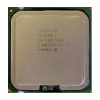
Related product manuals