Datasheet 49
Intel
®
Celeron
®
Processor up to 1.10 GHz
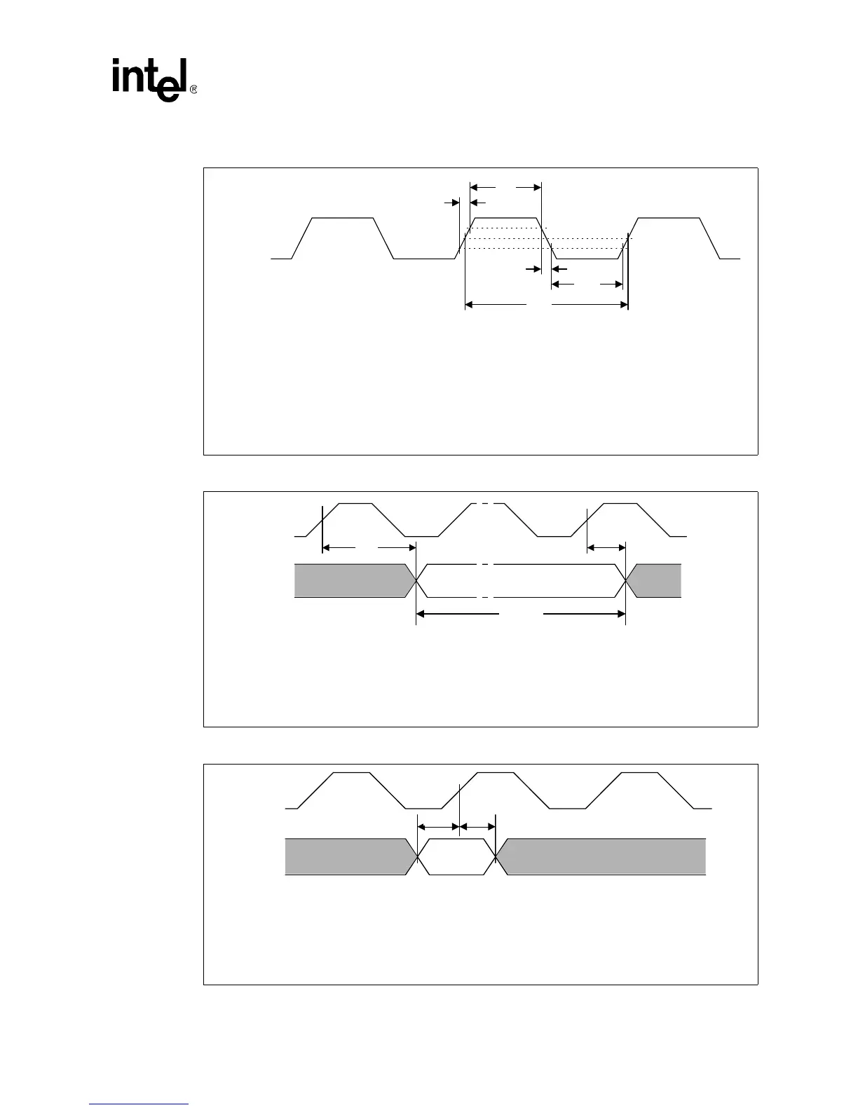
Figure 3. BCLK*, PICCLK, and TCK Generic Clock Waveform
Figure 4. System Bus Valid Delay Timings
Figure 5. System Bus Setup and Hold Timings
Note: BCLK is referenced to 0.5 V and 2.0 V. PICCLK is referenced to 0.7 V and 1.7 V.
For S.E.P. and PPGA packages, TCK is referenced to 0.7 V and 1.7 V.
For the FC-PGA package, TCK is referenced to V
REF
±200mV.
1.7V (2.0V*)
1.25V
0.7V (0.5V*)
t
r
t
p
t
f
t
h
t
l
CLK
T
r
= T5, T25, T34 (Rise Time)
T
f
= T6, T26, T35 (Fall Time)
T
h
= T3, T23, T32 (High Time)
T
l
= T4, T24, T33 (Low Time)
T
p
= T1, T22, T31 (BLCK, TCK, PICCLK Period)
V = 1.0V for AGTL+ signal group;
For S.E.P and PPGA packages, 1.25V for CMOS, APIC and JTAG signal groups
For FC-PGA package, 0.75V for CMOS, APIC and TAP signal groups
CLK
Signal
Valid Valid
Tx
V
Tx
Tpw
Tx = T7, T11, T29a, T29b (Valid Delay)
Tpw = T14, T14B, T15 (Pulse Width)
CLK
Signal
Valid
Ts
V
Th
Ts = T8, T12, T27 (Setup Time)
Th = T9, T13, T28 (Hold Time)
V = 1.0V for AGTL+ signal group;
For S.E.P. and PPGA packages, 1.25V for APIC and JTAG signal groups
For the FC-PGA package, 0.75V for APIC and TAP signal groups